For CT-2
| Created by | Borhan |
|---|---|
| Last edited time | |
| Tag |
Topic 01: Fiber Fabrication
Definition: Fiber Fabrication is the process of manufacturing long, thin, flexible strands (optical fibers) made of high-purity glass (silica) to guide light signals over long distances with minimal loss.
1. Materials for Fiber Fabrication
Starting Materials:
- Main Material: Silica (SiO₂), derived from Silicon Tetrachloride (SiCl₄).
- Dopants (to modify properties):
- GeCl₄ (Germanium Tetrachloride): Increases refractive index.
- TiCl₄ (Titanium Tetrachloride): Enhances specific optical properties.
- BBr₃ (Boron Tribromide): Decreases refractive index.
- Purity Requirement: Transition metals (e.g., iron, copper) must be below 10 ppb (parts per billion) to avoid light absorption, which weakens the signal.
Mnemonic: "SGTB" (Silica, Germanium, Titanium, Boron) – Think of a Super Glass Tower Base to remember the key materials.
Process: Gaseous halides of silica and dopants are combined in Vapor Phase Oxidation.
2. Vapor Phase Oxidation
Converts gaseous materials into solid glass particles (soot) for fiber production. Two methods:
- Flame Hydrolysis: Uses flame to oxidize gases into soot.
- Chemical Vapor Deposition (CVD): Deposits soot inside a tube or on a surface.
Mnemonic: "Flaming CVD" – Picture a flame (Flame Hydrolysis) and a chemical vapor cloud (CVD) creating glass soot.
3. Types of Glass Used in Fiber Fabrication
| Material | Use | Properties |
| Silica (SiO₂) | Most common for optical fibers | Low loss, ideal for telecom |
| Fluorozirconate/Fluoroaluminate | Special fibers | Good for infrared transmission |
| Chalcogenide Glasses | Long-wavelength infrared | High Refractive Index (RI ≈ 3.0) |
| Crystalline Materials (e.g., Sapphire) | Special applications | Durable, infrared transmission |
Mnemonic: "SFCC" – Silica, Fluoride, Chalcogenide, Crystalline. Imagine a Shiny Fiber Cable Core to recall these materials.
4. Refractive Index (RI)
- Silica/Fluoride Glasses: RI ≈ 1.5 (moderate).
- Chalcogenide Glasses: RI ≈ 3.0 (very high).
- Core vs. Cladding: RI difference is kept < 1% to ensure Total Internal Reflection, preventing light leakage.
Mnemonic: "1.5 for Silica, 3 for Chalcogenide" – Think "1.5 = Simple Silica, 3 = Complex Chalcogenide".
5. Basic Principle of Fiber Fabrication
- Process: Chemical reactions produce oxides (e.g., SiO₂), deposited as glass layers on a substrate (glass rod/tube) or inside a hollow tube via successive layering.
- Dopant Control: Gradually adjust dopant concentration to create desired Refractive Index Profile (e.g., graded index for specific fibers).
- Output: A solid glass rod or hollow tube, collapsed into a preform (a thick glass rod).
Mnemonic: "Layer, Dopant, Preform" – Imagine layering dough, adding spices (dopants), and baking a preform loaf.
6. Silica in Fiber Fabrication
- Why Silica?
- Excellent optical transmission, especially in near-infrared (1.55 µm or 1550 nm).
- Low absorption and scattering (~0.2 dB/km loss).
- Achieved using ultra-pure silica.
Mnemonic: "Silica Shines at 1550" – Picture silica as a shiny star glowing brightest at 1550 nm.
7. Silica Glass Fiber: Fiber Fabrication Process (Two Stages)
- Preform Fabrication: Create a thick glass rod with precise refractive index profile.
- Fiber Drawing: Heat and pull the preform into thin fiber.
Stage 1: Preform Fabrication
Method: Chemical Vapor Deposition (CVD), specifically Inside Vapor Deposition.
- Steps:
- Use a hollow glass tube (~40 cm long) as a substrate, rotated in a lathe.
- Inject SiCl₄ + O₂ (and dopants like GeCl₄) into the tube.
- Heat with a hydrogen burner (~1600°C) to form SiO₂ soot (fine glass particles).
- Soot deposits on the tube’s inner surface (soot deposition).
- Gradually build layers, adding dopants to form core (higher RI) and cladding (lower RI).
- Heat to 2000°C to collapse the tube into a solid preform rod.
Core vs. Cladding Techniques:
| Technique | Core Material | Cladding Material |
| Technique 1 | Doped SiO₂ (Ge, Al, P, Ti) | Pure SiO₂ |
| Technique 2 | Pure SiO₂ | Doped SiO₂ (F, B) |
Mnemonic: "Soot to Solid" – Think of soot piling up inside a tube, then solidifying into a preform rod.
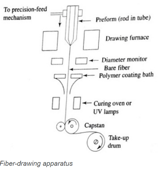
Stage 2: Fiber Drawing Process
Steps:
- Place preform in a Drawing Tower.
- Heat the preform’s tip (~2000°C) using a gas burner or graphite heater until it softens.
- Pull the softened glass into a thin fiber (like pulling taffy).
- Monitor fiber diameter with a Diameter Monitor to maintain ~125 µm, adjusting pulling speed.
- Apply UV-curable polymer coating to protect the fiber.
- Cure coating with UV light.
- Use a Capstan to control pulling speed/tension.
- Wind the fiber onto a Take-up Reel.
Mnemonic: "Heat, Pull, Coat, Reel" – Imagine heating a candy rod, pulling it thin, coating it with chocolate, and reeling it up.
8. Liquid Phase (Melting) Method (Rod-in-Tube Method)
Steps:
- Create a core glass rod (for light transmission).
- Insert the rod into a cladding glass tube to form a preform.
- Heat the preform in a drawing furnace (~2000°C).
- Pull into a thin fiber (~125 µm diameter).
- Monitor diameter and adjust pulling speed.
- Apply polymer coating, cure with UV light.
- Wind onto a reel.
Note:
- A 1-meter preform yields 20-30 km of fiber in 2-3 hours.
- Limitation: Batch process, not suitable for continuous production.
Mnemonic: "Rod in Tube, Heat, Pull" – Picture a rod sliding into a tube, heated, and pulled like a straw.
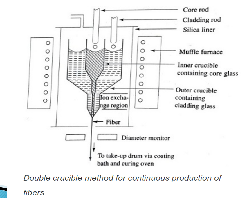
9. Double Crucible Method
Use: Continuous fiber manufacturing.
Setup: Two concentric platinum crucibles in a muffle furnace (800-1200°C).
Steps:
- Place core glass in the inner crucible, cladding glass in the outer crucible.
- Heat to melt both glasses.
- Molten glass flows through nozzles at the crucible bottoms, forming a core-cladding fiber.
- Apply polymer coating and wind onto a reel.
- Achieve graded index via dopant diffusion between core and cladding.
Mnemonic: "Double Crucible, Melt, Flow" – Imagine two nested pots melting glass, flowing out like syrup into a fiber.
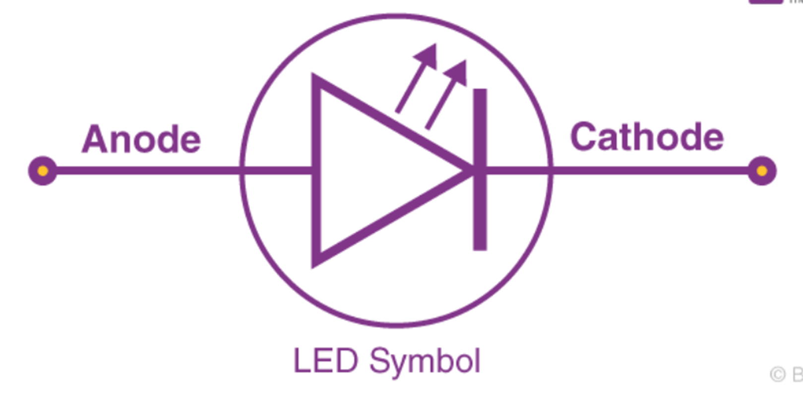
Topic 02: Light Emitting Diode (LED)
1. Definition of LED
An LED (Light Emitting Diode) is a semiconductor p-n junction device that emits light when forward-biased. It converts electrical energy into optical energy through electron-hole recombination.
- It emits light only when forward biased.
- Commonly used in communication and display systems.
Mnemonic:
"LED = Light Emission through Drift"
- L → Light
- E → Electron-hole recombination
- D → Drift in forward bias
2. Working Principle of LED
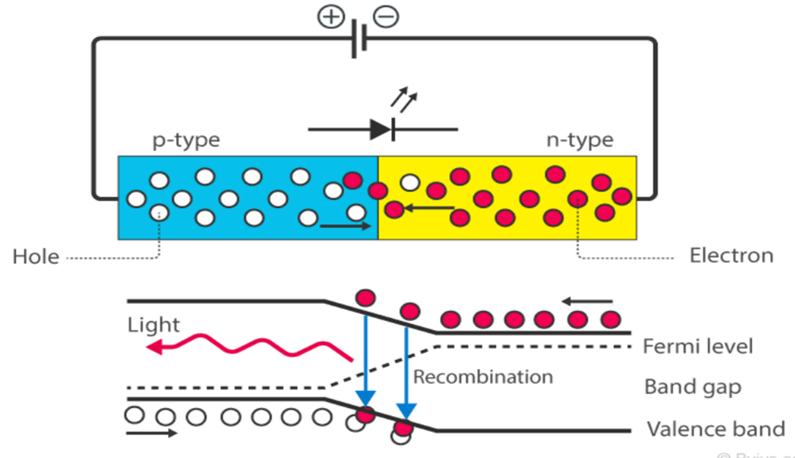
- When forward biased, electrons move from the n-region to p-region, and holes move from p to n.
- At the junction, they recombine.
- This recombination releases energy in the form of photons (light).
- The color of the emitted light depends on the bandgap energy of the semiconductor.
3. Quantum Theory and LED
According to quantum theory:
- When an electron jumps from a higher energy level (conduction band) to a lower level (valence band), it emits a photon.
Formula:
Where:
= Bandgap energy (Joules)
= Planck’s constant =
= Frequency of emitted light (Hz)
= Wavelength of emitted light (m)
= Speed of light =
Key point:
- Wavelength λ is inversely proportional to energy gap Eg
4. Why LEDs Use Compound Semiconductors (Not Si or Ge)
- Silicon (Si) and Germanium (Ge) are indirect bandgap semiconductors.
- Electron-hole recombination does not produce visible light.
- Energy is emitted as heat or infrared radiation.
- LEDs require direct bandgap semiconductors (e.g., GaAs, GaP) to emit visible photons.
5. Steps of LED Operation
| Step | Description |
| 1 | Apply forward bias voltage |
| 2 | Electrons and holes recombine |
| 3 | Photon (light) is emitted |
| 4 | Photon energy is E=hcλE = \frac{hc}{\lambda}E=λhc |
Mnemonic:
"BREE" → Bias, Recombine, Emit, Energy
6. LED Biasing Circuit
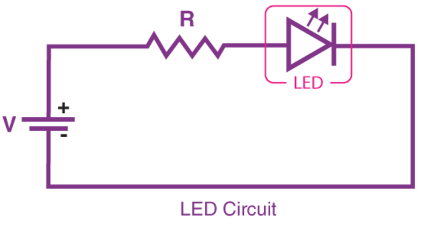
- LEDs require current-limiting resistors to avoid excessive current.
- Operating voltage: 1V to 3V
- Operating current: 20 mA to 100 mA
Formula for current:
Where:
- I_F = Forward current
- V_s = Source voltage
- V_D = LED voltage drop
- R_s = Series resistor
Mnemonic:
"IF = V over R" – Apply Ohm’s Law
7. Materials Used and LED Colors
| Material | Emitted Color |
| GaAs | Infrared |
| GaAsP | Red, Orange |
| AlGaAsP | Bright Red, Orange, Yellow |
| GaP | Red, Yellow, Green |
| AlGaP | Green |
| GaN | Green, Emerald Green |
| GaInN | Blue-Green, Blue, UV |
| SiC | Blue (substrate) |
| ZnSe | Blue |
| AlGaN | Ultraviolet |
Mnemonic:
"Great Artists Always Paint Green Gardens In Soft Zonal Areas"
8. Differences Between Diode and LED
| Feature | Diode | LED |
|---|---|---|
| Purpose | Conduct current | Emit light |
| Emission | None | Visible/Infrared light |
| Material | Si, Ge | GaAs, GaP, etc. |
| Application | Rectifiers, switches | Indicators, displays |
| Light Source | No | Yes |
Mnemonic:
"Diode for Direction, LED for Light"
9. Important Characteristics of LEDs
| Property | Value |
|---|---|
| Operating Voltage | 1V – 3V |
| Operating Current | 20 mA – 100 mA |
| Response Time | Very fast (ns) |
| Works in | Forward bias only |
| Light Emission | Photon-based |
| Color Determination | By bandgap |
10. Advantages of LEDs
- Compact size and low cost
- Low power consumption
- High efficiency
- Long life : Up to 50,000–100,000 hours.
- Instant on/off: No warm-up time, instant on/off.
- Environmentally friendly: Minimal harmful materials (e.g., no mercury).
- Operates well at low temperature
- Directional light
- Controllable brightness : Vivid, accurate colors.
- High reliability
Mnemonic:
"SPEED COLD LIFE"
- S: Small size
- P: Power efficient
- E: Eco-friendly
- E: Easily controlled
- D: Directional
- C: Color quality
- O: On instantly
- L: Long life
- D: Durable
- E: Economical
11. Disadvantages of LEDs
- Temperature sensitive
- Light quality may vary
- Efficiency drops at high voltage
- Must use correct polarity
- Sensitive to overheating
- Some colors attract insects
Mnemonic:
"TEMPLED"
- T: Temperature sensitive
- E: Efficiency drops
- M: May vary in color
- P: Polarity-sensitive
- L: Light attracts insects
- E: Easily damaged by heat
- D: Degrades with time
12. Applications of LEDs
- Residential and industrial lighting
- Mobile and laptop screens
- Digital displays and signboards
- Traffic lights
- Television displays
- Automotive headlights and tail lights
- Optical communication (fiber)
- Remote control indicators
Mnemonic:
"LED MOTORS"
- L: Lighting
- E: Electronics
- D: Display
- M: Motor vehicle lights
- O: Outdoor signage
- T: Traffic signals
- R: Remote indicators
- S: Screens and monitors
Topic 03: Laser Diode
Definition: A Laser Diode (LD), also known as a Semiconductor Laser, Junction Laser, or Injection Laser, is an optoelectronic device that converts electrical energy into a coherent light beam via stimulated emission. It is small, cost-effective, and widely used in optical communication.
Mnemonic: "LD = Little Laser Dynamo" – Picture a tiny dynamo producing a powerful laser beam.
1. Working Principles of Laser Diode
Laser diodes operate based on three fundamental principles:
a. Stimulated Emission
- Process: An incoming photon stimulates an excited electron to drop to a lower energy state, releasing a second photon with the same wavelength, phase, and direction.
- Result: One photon generates two photons, amplifying light to produce a coherent beam.
- Contrast with Other Emissions:
- Stimulated Absorption: Electrons absorb external energy (e.g., DC voltage) and jump to the conduction band.
- Spontaneous Emission: Excited electrons naturally drop to a lower state, emitting random photons.
Mnemonic: "Stimulated = Twin Photon Team" – Imagine one photon teaming up to create a twin, amplifying light.
b. Population Inversion
- Definition: A state where the number of electrons in a higher energy state (conduction band) exceeds those in the lower energy state (valence band).
- Importance: Essential for more stimulated emission than absorption, enabling light amplification.
- Achieved By: Pumping energy (e.g., electrical current) into the gain medium.
Mnemonic: "Population Inversion = Excited Electron Majority" – Picture a majority of electrons excited at a high-energy party.
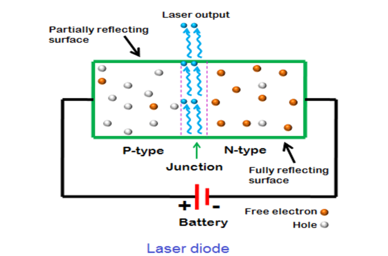
c. Cavity Resonance
- Description: The laser diode has an optical cavity with two reflective surfaces: one fully reflective (100%) and one partially reflective (~95%).
- Function: Photons bounce between mirrors, triggering more stimulated emission, amplifying light.
- Output: A narrow, high-intensity beam escapes through the partially reflective mirror.
Mnemonic: "Cavity = Mirror Bounce Booster" – Imagine light bouncing between mirrors to boost intensity.
Extra Info: Some lasers (e.g., nitrogen laser) produce a beam with a single pass through the gain medium, but most laser diodes require a cavity for sustained lasing.
2. Types of Emission
| Type | Description |
|---|---|
| Stimulated Absorption | Electrons absorb external energy and jump to the conduction band. |
| Spontaneous Emission | Excited electrons naturally recombine with holes, emitting random photons. |
| Stimulated Emission | An external photon triggers recombination, producing two photons with identical phase and direction. |
Mnemonic: "ABS: Absorb, Spark, Stimulate" – Absorb energy, Spark randomly, Stimulate coherently.
3. Steps of Laser Diode Operation
- Energy Absorption:
- DC voltage excites electrons from the valence band to the conduction band, creating holes in the valence band.
- Spontaneous Emission:
- Some electrons recombine with holes, emitting random photons.
- Stimulated Emission:
- Spontaneous photons stimulate other excited electrons to recombine, producing two photons per incident photon.
- Photons bounce between reflective surfaces, amplifying light.
- Light Output:
- A coherent, high-intensity beam escapes through the partially reflective mirror.
Mnemonic: "Absorb, Spark, Stimulate, Beam" – Absorb energy, Spark photons, Stimulate more, Beam out.
4. LED vs. Laser Diode
| Feature | LED | Laser Diode |
|---|---|---|
| Light Type | Incoherent | Coherent |
| Bandgap | Indirect/Direct | Direct |
| Light Propagation | Diffused | Directional, concentrated |
| Intensity | Low | Very high |
| Applications | Indicator lights, displays | CD/DVD drives, fiber optics |
| Cost | Cheaper | More expensive |
Mnemonic: "LED Diffuses, LD Directs" – LEDs scatter light, LDs shoot a direct beam.
Extra Info: Laser diodes use direct bandgap semiconductors (e.g., GaAs) for efficient photon emission, unlike LEDs, which may use indirect bandgap materials.
5. Population Inversion
- Definition: Occurs when more electrons are in the excited state than the ground state, essential for laser light production.
- Mechanism: Achieved by supplying external energy (e.g., current) to excite electrons.
Mnemonic: "PI = Pumped-Up Electrons" – Picture pumping electrons to a higher state.
6. Cavity Resonance and Optical Resonator
- Structure: Two mirrors form an optical cavity:
- Fully reflective (100%) mirror reflects all light.
- Partially reflective (~95%) mirror allows some light to escape as a laser beam.
- Process: Photons bounce multiple times, triggering stimulated emission, amplifying light exponentially when gain > loss.
- Lasing Threshold: The minimum pump power needed to overcome cavity losses and start lasing.
- Gain Saturation: As beam power increases, each stimulated emission returns atoms to the ground state, reducing gain until equilibrium is reached (in continuous wave lasers).
Mnemonic: "Resonator = Reflective Ping-Pong" – Light plays ping-pong between mirrors to amplify.
Extra Info: The cavity ensures only specific wavelengths (resonant modes) are amplified, contributing to the laser’s monochromaticity.
7. Gain Medium
- Definition: The material (e.g., p-n junction in GaAs) that amplifies light via stimulated emission.
- Process: Absorbs pump energy (e.g., electrical current), exciting electrons to higher energy states, which then emit coherent photons.
Mnemonic: "Gain = Glowing Active Material" – Picture the active medium glowing with amplified light.
8. Laser Light Characteristics
| Characteristic | Description |
|---|---|
| Coherence | Photons have identical phase and direction. |
| Monochromaticity | Single wavelength (one color). |
| Directionality | Narrow, straight beam with minimal spreading. |
| High Intensity | Extremely powerful light output. |
- Beam Types: Gaussian, top-hat, Bessel, multimode transverse modes, optical vortex.
Mnemonic: "CMDI = Coherent, Mono, Directional, Intense" – Think CMDI Laser Beam.
Extra Info: The coherence and directionality make laser diodes ideal for optical communication, ensuring minimal signal loss over long distances.
9. Fabry-Pérot Laser Diode
- Definition: The most common laser diode, using a Fabry-Pérot interferometer (two flat mirrors) as the resonator.
- Structure: A cavity with two mirrors creating standing waves for specific frequencies (longitudinal modes).
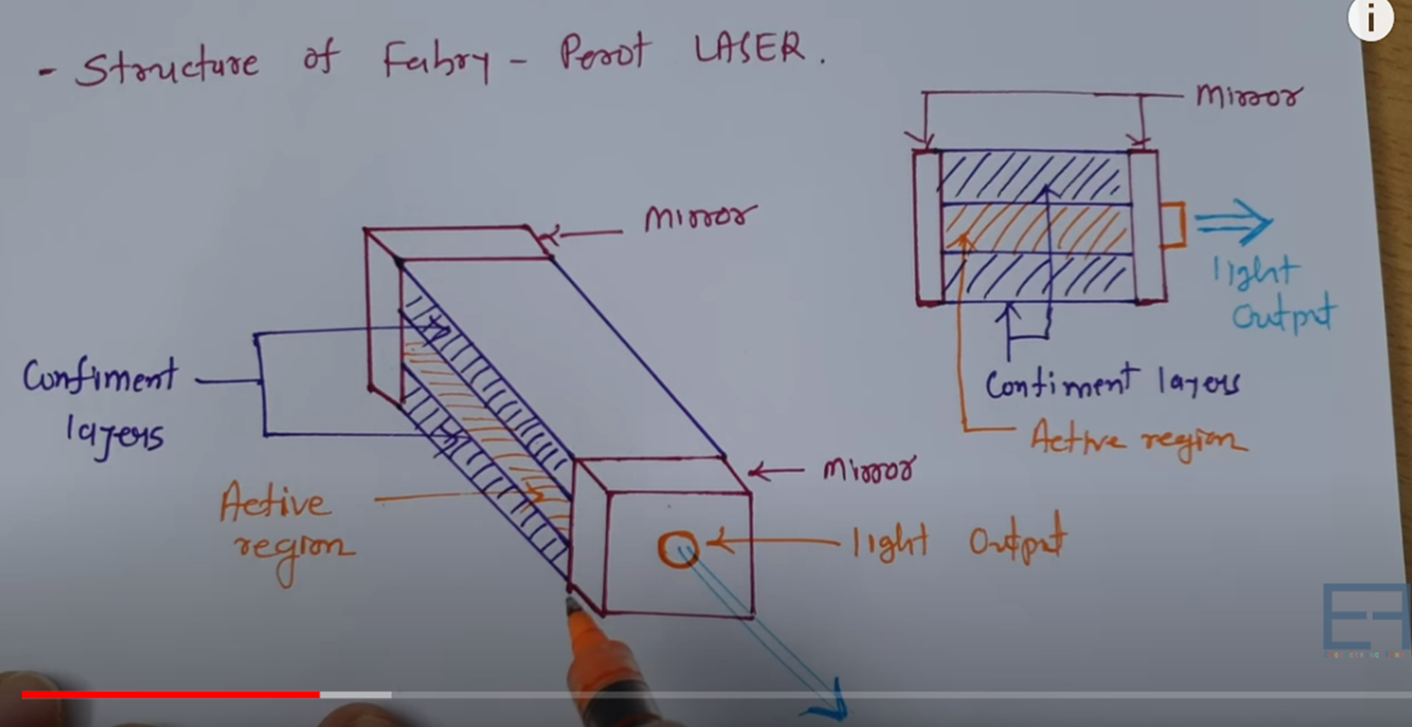
- Resonance Condition:
Where:
- f_n: nth harmonic frequency
- v: Speed of light in the medium
- L: Cavity length
- n: Mode number (integer)
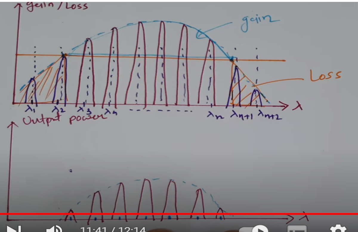
- Operation: Only frequencies that form standing waves (integral multiples of half-wavelength) are amplified, producing lasing modes.
- Note: May produce multiple longitudinal modes, requiring stabilization for high-speed communication.
Mnemonic: "Fabry-Pérot = Flat Mirror Waves" – Picture flat mirrors creating standing waves.
Extra Info: The gain spectrum overlaps with resonant frequencies, determining which modes lase. Stabilization techniques (e.g., distributed feedback) can reduce multiple modes.
10. How Laser Diode Works
- DC Voltage Application: Electrons move from n-type to p-type, becoming excited.
- Spontaneous Emission: Some electrons recombine, emitting random photons.
- Stimulated Emission: Photons stimulate more recombination, producing coherent photons.
- Photon Bouncing: Photons bounce between mirrors, amplifying via stimulated emission.
- Laser Output: A coherent beam escapes through the partially reflective mirror.
Mnemonic: "Volt, Spark, Stimulate, Bounce, Beam" – Voltage sparks, stimulates, bounces, beams.
11. Advantages and Disadvantages
| Advantages | Disadvantages |
|---|---|
| Simple construction | Not suitable for high-power applications |
| Lightweight | Highly temperature-sensitive |
| Cost-effective | — |
| Small size | — |
| Long lifespan | — |
| High efficiency | — |
| No external mirrors needed | — |
Mnemonic: "SLICE = Simple, Light, Inexpensive, Compact, Efficient" – Picture a slice of efficient laser tech.
Disadvantages: "Low Temp" – Low power, Temperature-sensitive.
Extra Info: Temperature control (e.g., thermoelectric coolers) is critical to maintain stable output and prevent degradation.
12. Applications of Laser Diode
- Optical disk drives (CD/DVD/Blu-ray)
- Barcode scanners
- Optical fiber communication
- Laser printers
- Medical instruments (e.g., eye surgery)
- Laser cutting and welding
- Laser pointers
- Military range-finding
- DNA sequencing
- Entertainment (laser shows)
Mnemonic: "FIBER-DISC" – Fiber optics, Instruments, Barcode, Entertainment, Range-finding, Disk drives, Surgery, Cutting.
Extra Info: In optical communication, laser diodes are preferred over LEDs due to their narrow spectral width and high modulation speed, enabling high data rates.
13. Additional Key Information for Exam
- Lasing Threshold: The minimum current required to achieve population inversion and start lasing. Below this, the LD emits incoherent light (like an LED).
- Gain Saturation: In continuous wave (CW) lasers, gain decreases as more atoms return to the ground state, stabilizing the output power.
- Materials: Typically gallium arsenide (GaAs) or related compounds, with doping agents like selenium, aluminum, or silicon.
- Response Time: Laser diodes have fast rise/fall times (nanoseconds), ideal for high-speed data transmission.
- Safety: Laser light can cause eye damage; proper precautions (e.g., shielding) are essential.
- Comparison with Gas Lasers: Laser diodes are smaller, cheaper, and more efficient than gas lasers (e.g., He-Ne), but have lower power output.
Topic: Photodiode
Definition: A Photodiode is an optical detector that converts light (photons) into an electrical signal (current). It is widely used in fiber optic communication, sensors, light measurement, and security systems.
Mnemonic: "Photodiode = Photon-to-Current Device" – Picture a device turning photons into a current flow.
1. Optical Detectors
- Definition: Devices that detect light and convert it into electrical signals.
- Applications: Fiber optic communication, sensors, light intensity measurement, security systems.
Mnemonic: "Optic Detectors = Light-to-Signal Machines" – Imagine light being transformed into signals.
Extra Info: Photodiodes are preferred in optical communication due to their high sensitivity and fast response, enabling reliable data detection.
2. p-n Photodiode
Definition
A p-n Photodiode is a p-n junction diode that generates a reverse current when exposed to light under reverse bias. The current increases with light intensity.
Mnemonic: "p-n = Photon-Triggered Current" – Picture photons triggering current in a p-n junction.
Structure and Working Principle
- Structure: A reverse-biased p-n junction diode.
- Process:
- When light hits the depletion region, it creates electron-hole pairs.
- The electric field in the depletion region separates electrons and holes, generating a photocurrent.
- Higher light intensity → more pairs → higher current and lower resistance.
- Light Interaction:
- Light in the depletion region produces photocurrent.
- Light in p or n regions (far from depletion) is lost as heat.
Key Characteristics
| Characteristic | Description |
|---|---|
| Responsivity | Ratio of generated current to incident light power (A/W). Varies with wavelength. |
| Dark Current | Small current produced without light, contributing to system noise. |
| Response Time | Time for charge carriers to cross the junction. Wider depletion region → faster response. |
| Breakdown Voltage | Maximum reverse voltage before the diode risks damage. |
Mnemonic: "RDRB = Responsivity, Dark, Response, Breakdown" – Think RDRB for p-n traits.
Applications
- Alarm circuits
- Counter circuits
- Computer interface devices
Extra Info: p-n photodiodes are cost-effective but have lower sensitivity compared to other types, making them suitable for basic applications.
3. p-i-n Photodiode
Definition
A p-i-n Photodiode has a p-type, intrinsic (i), and n-type region, with the intrinsic layer increasing the depletion region size, improving speed and efficiency.
Mnemonic: "p-i-n = Photon-Intrinsic Powerhouse" – Picture an intrinsic layer boosting photon detection.
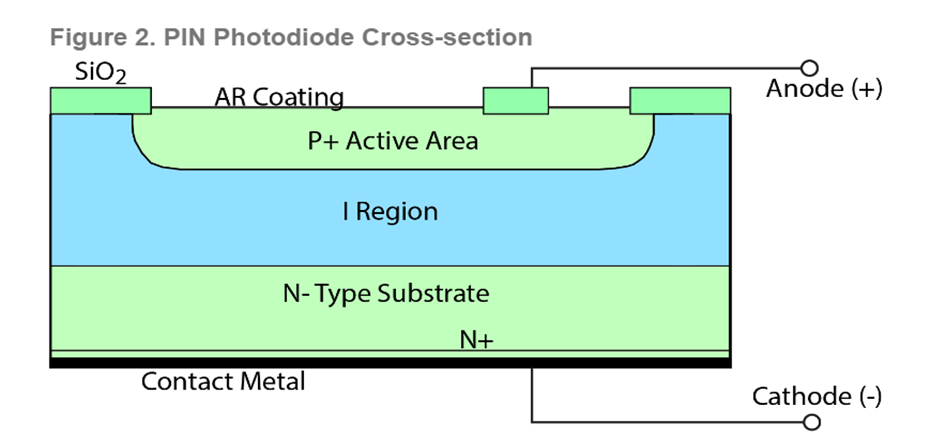
Structure and Working Principle
- Structure: p-type, thin intrinsic (undoped) layer (10–200 µm, high resistance), n-type.
- Process:
- The intrinsic layer enhances light absorption, generating more electron-hole pairs.
- Larger depletion region reduces capacitance and increases responsivity.
- Reverse bias enhances charge carrier separation, producing higher photocurrent.
Key Characteristics
| Characteristic | Description |
|---|---|
| High Response Speed | Large intrinsic region enables fast operation. |
| Low Capacitance | Intrinsic layer reduces capacitance, improving speed. |
| High Quantum Efficiency | More photons convert to electrons, enhancing efficiency. |
Mnemonic: "SRF = Speedy, Reduced-Capacitance, Efficient" – Think SRF for p-i-n perks.
Applications
- Fiber optic communication
- X-ray and gamma-ray detection
- RF and microwave circuits
- Photovoltaic cells and photodetectors
Additional Info
- Reverse Bias: Acts as a variable capacitor.
- Forward Bias: Acts as a variable resistor.
Extra Info: The intrinsic layer makes p-i-n photodiodes ideal for high-speed applications like optical receivers in fiber optic systems due to their low capacitance and fast response.
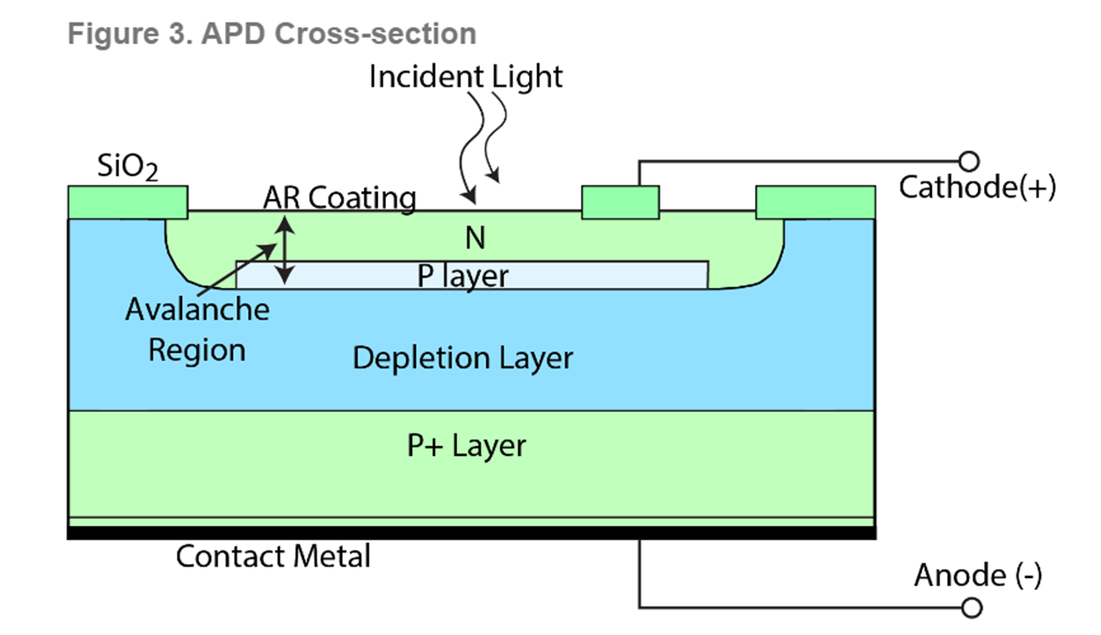
4. Avalanche Photodiode (APD)
Definition
An Avalanche Photodiode (APD) is a highly sensitive photodiode that uses the avalanche effect to multiply the photocurrent, producing significant current even with weak light.
Mnemonic: "APD = Avalanche Power Detector" – Picture an avalanche of electrons amplifying light detection.
Structure and Working Principle
- Structure: Includes p+, p, intrinsic (i), n, n+ regions.
- Process:
- Under high reverse bias (near breakdown), light generates electron-hole pairs.
- These carriers gain energy in a strong electric field, causing impact ionization (collisions create more pairs).
- This results in internal gain, amplifying the photocurrent significantly.
- Impact Ionization: Electrons accelerate, collide with atoms, and generate additional electron-hole pairs, creating a multiplication effect.
Key Characteristics
| Characteristic | Description |
| High Internal Gain | Avalanche effect multiplies current significantly. |
| High Responsivity | Produces large current from minimal light. |
| High Speed | Low transit time ensures fast response. |
| Higher Noise | Impact ionization increases noise, but signal-to-noise ratio remains good. |
Mnemonic: "GRIN = Gain, Responsivity, Intense, Noisy" – Think GRIN for APD traits.
Applications
- Weak light detection
- Fiber optic receivers
- Laser range finders
- Nuclear detection
Extra Info: APDs are used in low-light conditions (e.g., long-distance fiber optic links) but require precise voltage control to avoid excessive noise or damage.
5. LED vs. Photodiode
| Feature | LED | Photodiode |
| Function | Emits light | Detects light |
| Bias | Forward bias | Reverse bias |
| Conversion | Electricity → Light | Light → Electricity |
| Applications | Lighting, displays | Sensors, communication |
| Sensitivity | Low | High |
Mnemonic: "LED Shines, Photodiode Senses" – LEDs shine light, photodiodes sense it.
6. Comparison: p-n, p-i-n, and Avalanche Photodiode
| Feature | p-n Photodiode | p-i-n Photodiode | Avalanche Photodiode (APD) |
| Structure | p and n regions | p, intrinsic, n regions | p+, p, intrinsic, n, n+ regions |
| Depletion Region | Small | Large (due to intrinsic layer) | Large with high electric field |
| Bias Type | Reverse bias | Reverse bias | High reverse bias (near breakdown) |
| Light Absorption | Low | High | Highest (due to avalanche effect) |
| Responsivity | Low | Medium | Very high (internal gain) |
| Internal Gain | None | None | Yes (avalanche multiplication) |
| Current Output | Low | Higher | Highest |
| Speed | Slow | Fast (low capacitance) | Very fast (but some noise) |
| Noise | Low | Medium | High (due to impact ionization) |
| Cost | Low | Medium | High |
| Applications | Light sensors, counters | Fiber optics, X-ray detectors | Weak light detection, range finders |
Mnemonic: "p-n Simple, p-i-n Speedy, APD Super-Sensitive" – Picture p-n as basic, p-i-n as fast, APD as ultra-powerful.
7. Tips for Memorization
- p-n Photodiode:
- Simple, cheap, low current.
- Mnemonic: "p-n = Plain and Normal" – Basic light detector.
- p-i-n Photodiode:
- Intrinsic layer boosts absorption and speed.
- Mnemonic: "p-i-n = Intrinsic Speed King" – Fast and efficient.
- Avalanche Photodiode:
- High gain, sensitive to weak light, but noisy.
- Mnemonic: "APD = Avalanche Powerhouse" – Amplifies like an avalanche.
8. Additional Key Information for Exam
- Responsivity Formula: R = I_ph / P_opt (A/W), where I_ph is photocurrent and P_opt is optical power.
- Quantum Efficiency: Percentage of photons converted to electron-hole pairs. Higher in p-i-n and APD due to larger depletion regions.
- Dark Current Causes: Thermal generation of carriers, surface leakage, or tunneling. Minimized with proper material selection.
- Noise in APDs: Due to random impact ionization. Excess noise factor quantifies this, impacting signal quality.
- Wavelength Sensitivity: Photodiodes are optimized for specific wavelengths (e.g., 850 nm, 1310 nm, 1550 nm in fiber optics).
- Safety: High reverse bias in APDs requires careful handling to prevent breakdown.