DLD QA
| Created by | Borhan |
|---|---|
| Last edited time | |
| Tag |
Digital System
Q:
- What is meant by digital systems? What are the advantages of digital techniques?
- What are the advantages of digital systems over analog systems?
- What are the advantages of digital technique over analog? What are the limitations?
- Write the advantages of digital system. Why does every digital system use the binary number system?
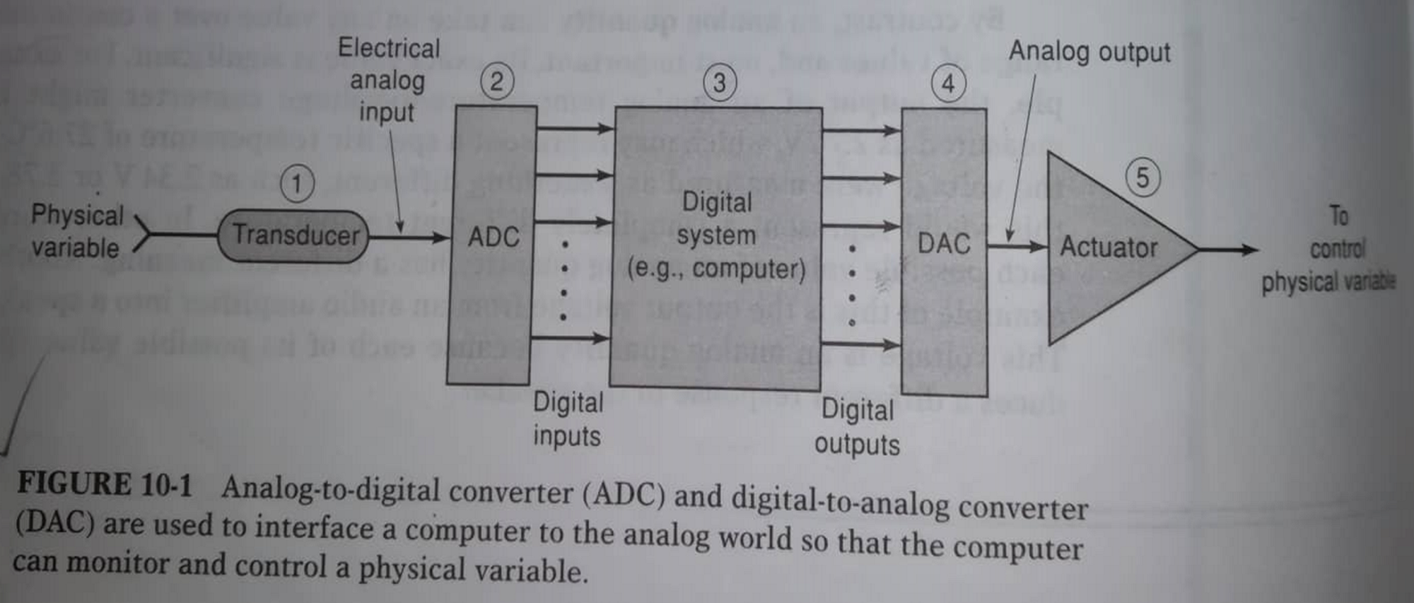
- Describe how analog-to-digital (ADC) converter and digital-to-analog (DAC) converter interface a computer to the analog world.
- What is meant by digital systems? What are the major differences between analog and digital system?
- Write some advantages of digital system.
- Describe how analog-to-digital (ADC) converter and digital-to-analog (DAC) converter are used to interface a computer to the analog world.
- Describe the analog to digital conversion technique using digital-ramp ADC circuit? (Skipped)
- What are the advantages of digital technique over analog? What are the limitations?
A:
- Digital systems refer to systems or devices that process, store, and transmit information in a digital format, typically using binary digits (bits) representing 0s and 1s. These systems rely on electronic circuits and components to perform various operations such as data manipulation, storage, and communication.
Advantages:
- Accuracy : highly accurate
- Flexibility : high level of flexibility in terms of processing and manipulating
- Storage : easily stored, retrieved, copied w/o losing quality
- Signal Processing : excel in processing signal by converting them digital representation
- Automation : can be easily automated, enabling the implementation of sophisticated control, decision making algorithm → enhances efficiency, productivity, reduces human intervention
Disadvantages:
- Conversion Loss : analog to digital
- Cost : expensive
- Complexity : complex design and specialized to develop and operate
- Sampling rate limitation : loss information if the sampling rate is not appropriately chosen
- Vulnerability to disruptions : rely on electricity → power outrage, hardware failure → system failure, data loss
- Every digital system uses the binary number system because it aligns with the fundamental nature of digital electronics and allows for efficient and reliable information processing.
- Simplicity : has only two digits, easy to implement in electronic circuit
- reliability : binary digits are less prone to errors and noise compared to analog, reducing misinterpretation during transmission and processing
- compatibility : the binary system is compatible with the basic logic operations of digital circuits
- scalability : the binary system scales well with the growth of digital system, easy to add more digits,
- Standardization : binary system has become de facto standard in digital system, it allows compatibility, consistency across different device, platforms and programming languages
- Mathematical simplicity : binary arithmetic is relatively simple compared to other number system
| Aspect | Analog System | Digital System |
|---|---|---|
| Data Representation | Continuous, varying physical quantities | Discrete, quantized values |
| Precision and Accuracy | Infinite precision, potential loss of accuracy | Precise and accurate representation, no loss due to noise |
| Signal Processing | Continuous mathematical operations | Discrete operations using algorithms and logical operations |
| Storage and Reproduction | Stored and reproduced directly in original form | Encoded in binary codes for storage and reproduction |
| Flexibility and Manipulation | Limited flexibility and manipulation | High flexibility and easy manipulation with software algorithms |
| Compatibility and Integration | Limited integration of different media types | Seamless integration of various media types |
| Signal Quality | Susceptible to degradation and interference | More resistant to noise and preserves signal quality |
| Applications | Audio processing, music production, specific sensors | Computers, telecommunications, image processing, data storage |
NAND and NOR gate
Q:
- What do you meant by universality of NAND gates and NOR gates?
- Show how a two-input NAND gale can be constructed from two-input NOR gates.
- Show how a two-input NAND gale can be constructed from two-input NOR gates.
- What do you meant by universality of NAND gates und NOR gates?
- Show how two-input NAND gate can be constructed from two-input NOR gates.
- What do you meant by universality of NAND gates and NOR gates? Show how a two input NAND gate can be constructed from two input NOR gate.
- How can a two-input NAND gate be constructed from two-input NOR gates?
- Describe the operation of basic TTL NAND gate logic circuit
- Implementing logical expression …. using only NAND gates?
- Implementing logical expression … using only NOR gates?
A:
- Universality : any logical expression can be implemented by using only NAND or NOR gate
The universality of NAND (Not-AND) gates and NOR (Not-OR) gates refers to the fact that these two types of logic gates can be used to implement any logical function. In other words, any other logic gate or combination of gates can be created using only NAND gates or only NOR gates.
FF
Q:
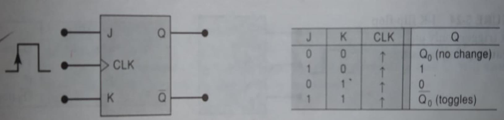
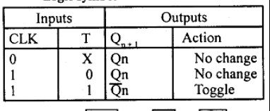
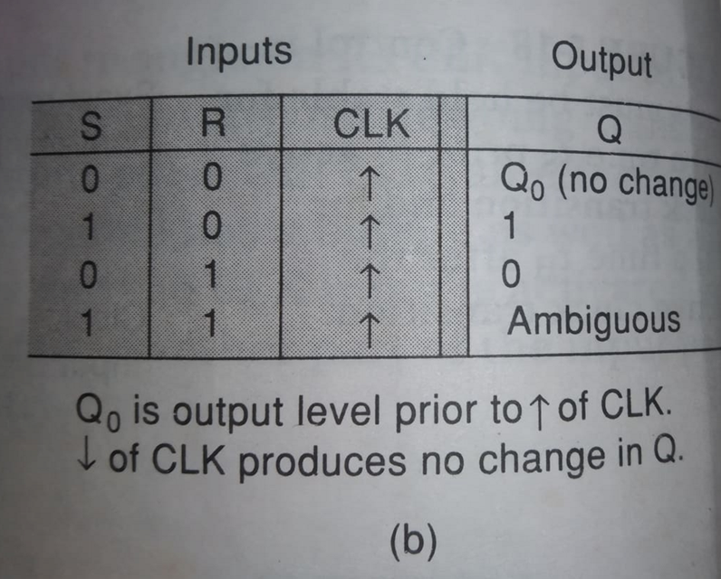
- What is FF? Differentiate between latch and FF.
- Compare between clocked J-K FF and clocked S-R FF
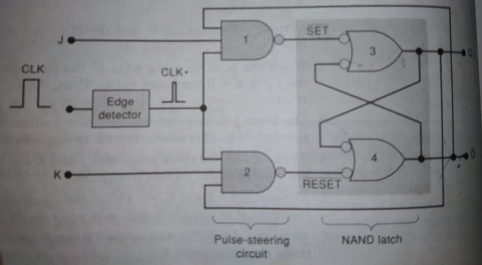
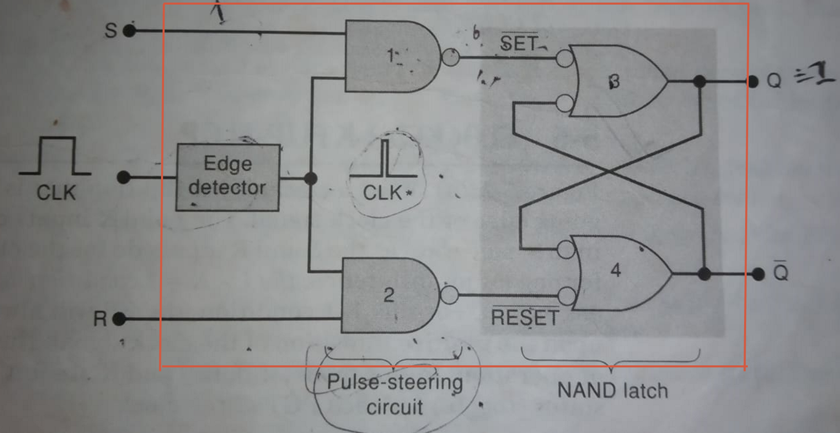
- Draw internal circuitry of the edge-triggered J-K.
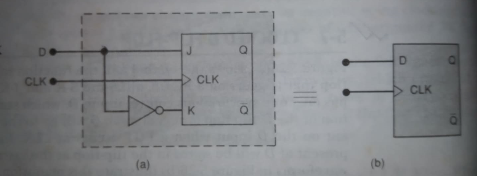
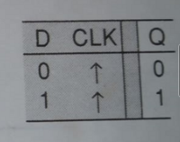
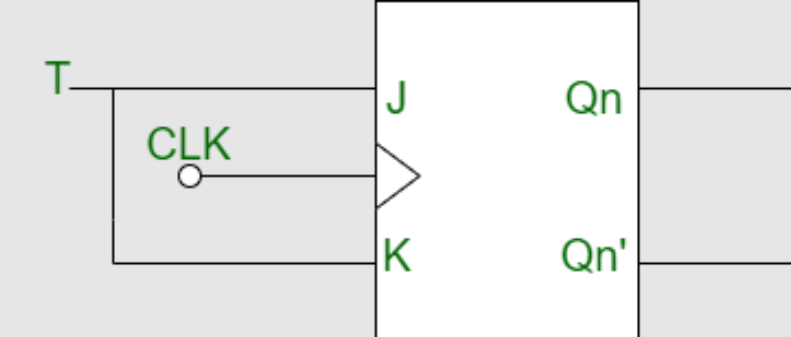
- Design D-FF and T-FF from J-K FF and describe with truth-tables.
- What is D flip-flop? How D flip-flop can be constructed using J-K flip-flop.
- Define Latch and FF. Draw the internal circuitry and truth table of the edge-triggered J-K
- Compare between clocked J-K FF and clocked S-R FF
- Explain the infernal circuitry of the Edge-Triggered S-C flip-flop. why the S and C inputs affect Q
only during the active transition of CLK.
- What is D flip-flop? How D flip-flop can be constructed using J-K flip-flop.
A:
- A Flip-Flop is a sequential logic circuit that is capable of storing one bit of information, which can be either a logic 0 or a logic 1. It is -11111commonly used as a building block in digital systems to store and manipulate binary data.
| Latch | Flip-Flop | |
|---|---|---|
| Definition | A latch is a level-sensitive sequential logic circuit used to store and maintain a binary state. | A flip-flop is a clocked sequential logic circuit used to store and control binary data |
| Type | Asynchronous | Synchronous |
| Enable Input | Yes | No |
| Sensitivity | Level-sensitive | Edge-sensitive |
| Clock Dependency | No clock input | Clock input required |
| Output Update | Immediate response to input changes | Updates at specific clock transitions |
| Output Stability | Output changes based on current inputs | Output changes based on clock edges |
| Applications | Small-scale circuits, building blocks, data storage | Processors, memory elements, state machines, register |
| Input Control | No clock signal required | Synchronized with a clock signal |
| States | Set and reset | Set, reset, and intermediate states |
| J-K Flip-Flop | S-R Flip-Flop | |
|---|---|---|
| Inputs | J (data input), K (data input), Clock | S (set input), R (reset input), Clock |
| Functionality | Stores and manipulates binary data | Stores and manipulates binary data |
| Operation | J-K inputs control the behavior of FF | S-R inputs control the behavior of FF |
| Feedback | Can have feedback (J and K connected to FF) | No feedback (S and R not connected to FF) |
| Forbidden State | None | S = 1, R = 1 results in an undefined state |
| Implementation | Can be implemented using logic gates | Can be implemented using logic gates |
| Applications | Counters, shift registers, memory elements | Memory elements, control circuits |
| Toggle State | Yes | No |
- A D flip-flop, also known as a data flip-flop or delay flip-flop, is a fundamental building block in digital logic circuits. It is a type of sequential logic circuit that stores and regulates the state of a single bit of information.
- A T flip-flop, also known as a toggle flip-flop, is a type of sequential logic circuit that can change its output state based on clock pulses.
BCD
Q:
- What is BCD code? What is an advantage of encoding a decimal number in BCD rather than in straight binary? What is a disadvantage?
- What is BCD code? What is an advantage of encoding a decimal number in BCD rather than in straight binary?
- What is BCD adder? When 0110 is added during BCD addition?
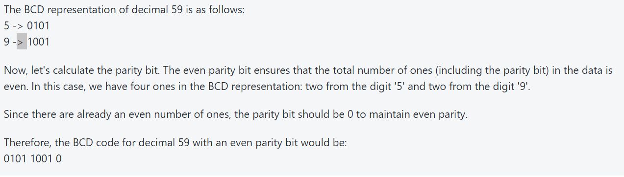
- What is a parity bit? Attach an even parity bit to the BCD code for decimal 59.
- What is BCD adder? When 0110 is added during BCD addition?
- Explain the operation of a BCD adder circuit that contains two four bit adders and a correction detector circuit.
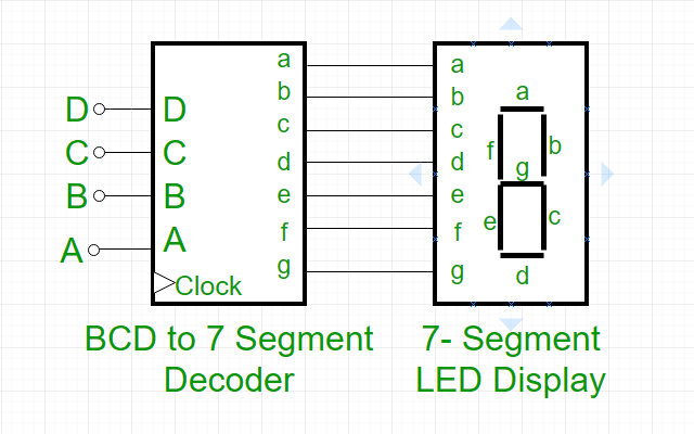
- What is decoder? Explain the operation of BCD to decimal decoders with logic diagram
- What is BCD to 7 segment decoder?
- Explain the operation of a BCD adder circuit that contains two or four bit adders and a correction detector circuit.
- Explain the operation of BCD counter.
- Explain the operation of a BCD adder circuit that contains two four bit adders and a correction
detector circuit.
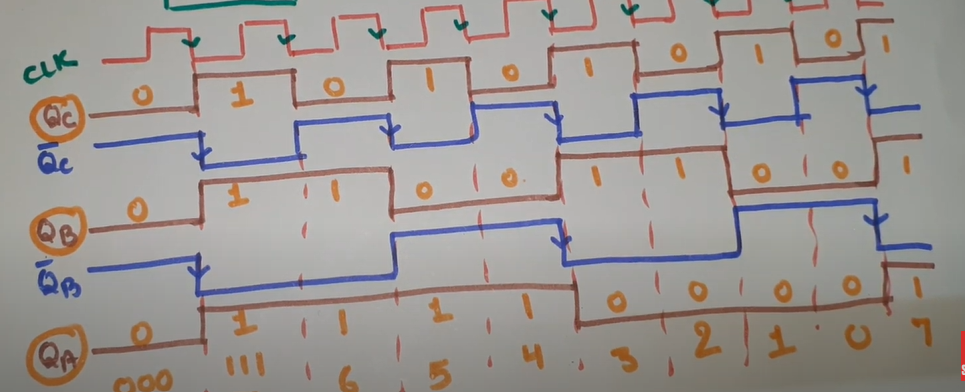
- Construct a BCD counter that counts 0000 through 1001. Explain its operation with necessary logic diagram and waveforms.
- What is decoder? Describe the common cathode BCD-to-7-segment decoder.
- Explain the operation of a BCD adder circuit that contains two four bit adders and a correction
detector circuit.
- Design a BCD-to-7 segment decoder and explain its operation to display decimal number ‘8’.
A:
- BCD is a binary representation of decimal numbers, where each decimal digit is encoded using a 4-bit binary code.
Advantage:
- No need any complex conversation algorithm
- Simplifying arithmetic operations
Disadvantage:
- Need more storage
- inefficient use of bits
- A BCD adder is a digital circuit capable of adding two BCD numbers together.
0110 is added when
- the sum is greater than 9
- when the carry bit creates another new bit
- A parity bit is a check bit, which is added to a block of data for error detection purposes.
- BCD adder
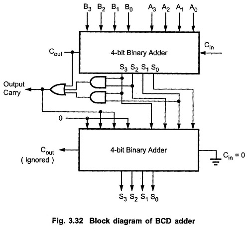
Four Bit BCD Adder Operation:
- There are two 4 bit BCD adder
- each 4 bit adder takes two BCD digits and produce a sum (4 bits) and a carry output
- How four bit added works
- adding two corresponding bits of the two BCD input and it generates a sum bit and a carry out bit for the next-higher-order-bit for each position
Correction Detector Circuit Operation
- examines the output of 4 bit adder and check if any of the resulting BCD digit are greater than 9, if it is, then it adds 6 (0110) to them
Design a 7 segment BCD counter
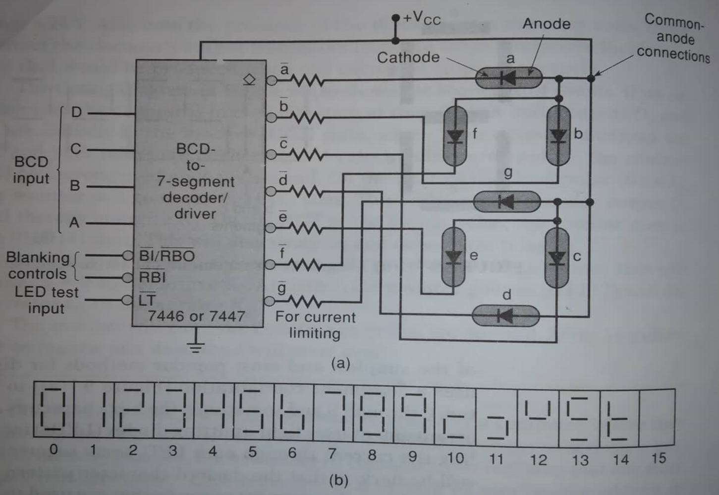
To print “8”
- BCD Input : 1000
- Decoder Operation :
- Set high to activate : a,b,c,d,e,f,g,h
- Display Operation:
- the activated output lines will turn on these segments
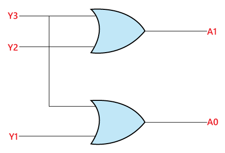
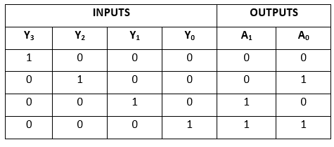
- A decoder is a combinational logic circuit that takes an input code and produces multiple output lines based on the input. It is commonly used in digital systems to convert a binary or coded input into a set of mutually exclusive output signals.
- BCD Counter Operation
- Initialization : the counter set to specific value, 0000
- Counting
- increment one by each clock pulse or input signal
- it cycle through 0-9
- Output
- at each count, the binary representation decoded to decimal and produce output
- Reset
- after reaching maximum value 9, it starts counting from 0 again
- BCD Counter

- A common cathode BCD-to-7-segment decoder is a digital circuit that converts Binary Coded Decimal (BCD) inputs into the appropriate control signals to display the corresponding decimal digits on a 7-segment display. In a common cathode configuration, all the cathode terminals of the seven segments in the display are connected together and shared as a common ground or "0" reference. Operations:
- BCD Input
- Logic Gates
- Control Signals
- Display Operations
Counter
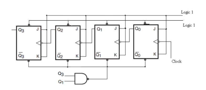
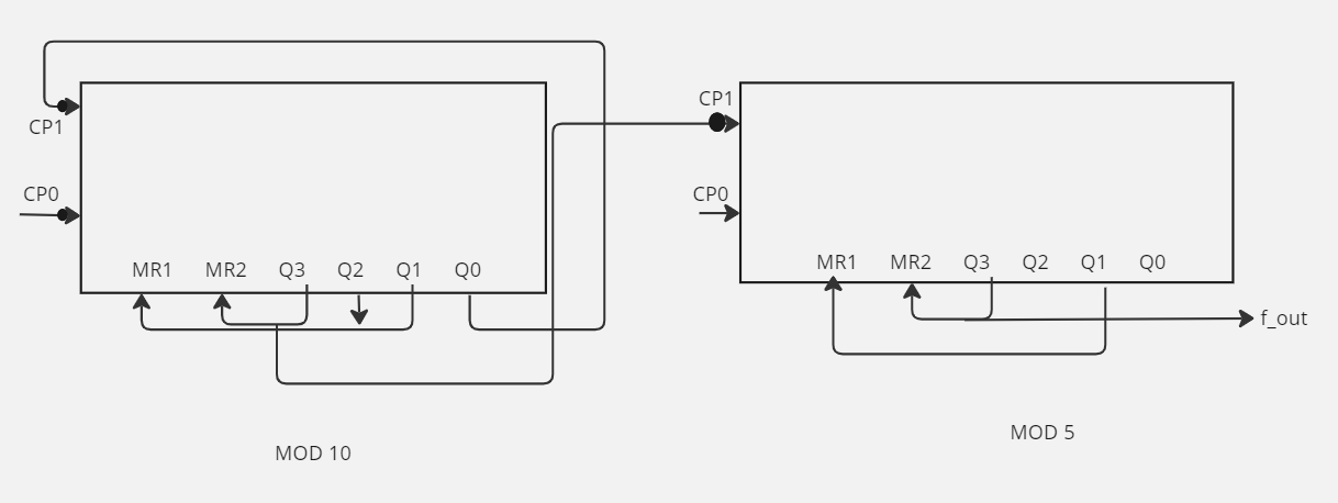
- Explain frequency division and counting operation using MOD-8 counter.
Frequency Division: Frequency division is a technique used to divide an input frequency by a certain factor to obtain a lower frequency output. The mod-8 counter divides by a factor of 8. That means, for every 8 input clock cycle, the counter will produce one output clock cycle. The output frequency is equal to the input frequency divided by 8.
Counting Operation: The MOD-8 counters starts from 0 to 7 and then reset back to 0.
- Considering the operation of MOD-8 counter answer the following.
- Why clock signal is applied in leftmost FF?
- LSB (probably)
- The leftmost FF receives the clock signal and triggers the counting sequence.
- Why J=K=1 applied?
- ensure the flip-flop toggles on each clock cycle
- Why all PRE=CLR=1?
- to disable their functionality
- When PRE=CLR=1, it ensures that the flip-flops are not preset or cleared during the counting operation.
- Why this counter is MOD-8?
- it has 8 unique states (0 to 7)
- Why this is named as counter?
- because it is designed to count and sequence through a specific range of numbers
- Why clock signal is applied in leftmost FF?
- What is the advantage of a synchronous counter over an asynchronous counter? What is
the disadvantage?Advantage:
- Speed
- Synchronization : making it easier to analyze and predict the behavior of the circuit.
- Modularity and scalability : more modularity and scalability than asynchronous
- Elimination of glitches : avoid the possibility of glitches,
- Error Rate : less error than asynchronous
Disadvantage:
- Complexity : more complex, require more logic gate
- Power Consumption : consume more power
- What is the difference between register and counter? Mention the differences between asynchronous and synchronous counter?
Aspect Register Counter Purpose a group of flipflop, stores a set of binary values a specific type of register, counts or keeps track of events/occurrences Data Storage Holds data for temporary storage or buffering Sequentially counts and stores the count value Operation Data can be loaded, stored, retrieved, and manipulated Counts up or down based on clock pulses or control signals Clock Inputs May or may not have a clock input Typically has a clock input to trigger counting Output Outputs the stored data Outputs the current count value Applications Used for temporary storage, data manipulation, and buffering Used for counting events, frequency division, timing, etc. Aspect Asynchronous Counter Synchronous Counter Clock Inputs Each flip-flop has its own clock input All flip-flops share a common clock input Timing Transition of flip-flops is independent and asynchronous Transition of flip-flops is synchronized and simultaneous Propagation Delay Accumulates due to independent clock inputs Negligible as all flip-flops transition together Glitches Prone to glitches due to timing discrepancies Glitches are eliminated due to synchronized transitions Design Complexity Relatively simpler design More complex design due to synchronization requirements Speed Slower operation due to propagation delay Faster operation due to simultaneous transitions Applications Less commonly used in high-speed systems Widely used in digital systems for reliable counting
- What is counter? Explain the mod-16 synchronous up/down counter.
Counter : A specific type register use to count or keep tract of events or occurrences
A mod-16 synchronous up/down counter is a type of counter that can count up or down in a sequence from 0 to 15 (or 15 to 0) using four flip-flops. It has two control inputs: an Up/Down control input and a clock input.
Here's a step-by-step explanation of how a mod-16 synchronous up/down counter works:
- Flip-Flop Configuration:
- Four D-type flip-flops are used, labeled as FF0, FF1, FF2, and FF3.
- Each flip-flop has two inputs: a data input (D) and a clock input (CLK).
- The outputs of the flip-flops are labeled as Q0, Q1, Q2, and Q3.
- Initial State:
- Initially, all flip-flops are reset to 0 (Q0 = Q1 = Q2 = Q3 = 0).
- Up/Down Control Input:
- The Up/Down control input determines the counting direction.
- When the Up/Down input is high (1), the counter counts up.
- When the Up/Down input is low (0), the counter counts down.
- Clock Input:
- The clock input triggers the transition of the counter from one state to another.
- The counter changes its state on the rising edge or falling edge of the clock signal, depending on the specific design.
- Counting Operation:
- When the Up/Down control input is high (1):
- On each rising edge (or falling edge) of the clock signal, the counter increments by 1 in a binary sequence.
- The counter goes through the states: 0000, 0001, 0010, 0011, ..., 1110, 1111, 0000, and so on.
- When the counter reaches 1111 (15 in decimal), it wraps around to 0000 and continues counting.
- When the Up/Down control input is low (0):
- On each rising edge (or falling edge) of the clock signal, the counter decrements by 1 in a binary sequence.
- The counter goes through the states: 1111, 1110, 1101, 1100, ..., 0010, 0001, 0000, 1111, and so on.
- When the counter reaches 0000, it wraps around to 1111 and continues counting down.
- When the Up/Down control input is high (1):
- Output:
- The outputs Q0, Q1, Q2, and Q3 represent the current count value in binary format.
- These outputs can be used for further processing or connected to other components in a digital system.
- Flip-Flop Configuration:
- Discuss the propagation delay in ripple counters.
In a ripple counter, the propagation delay refers to the delay between the input signal change and the corresponding output change as the signal ripples through the flip-flops in the counter.
- Construct a MOD-50 counter using IC 7415293. (Not sure about the answer whether correct or not)
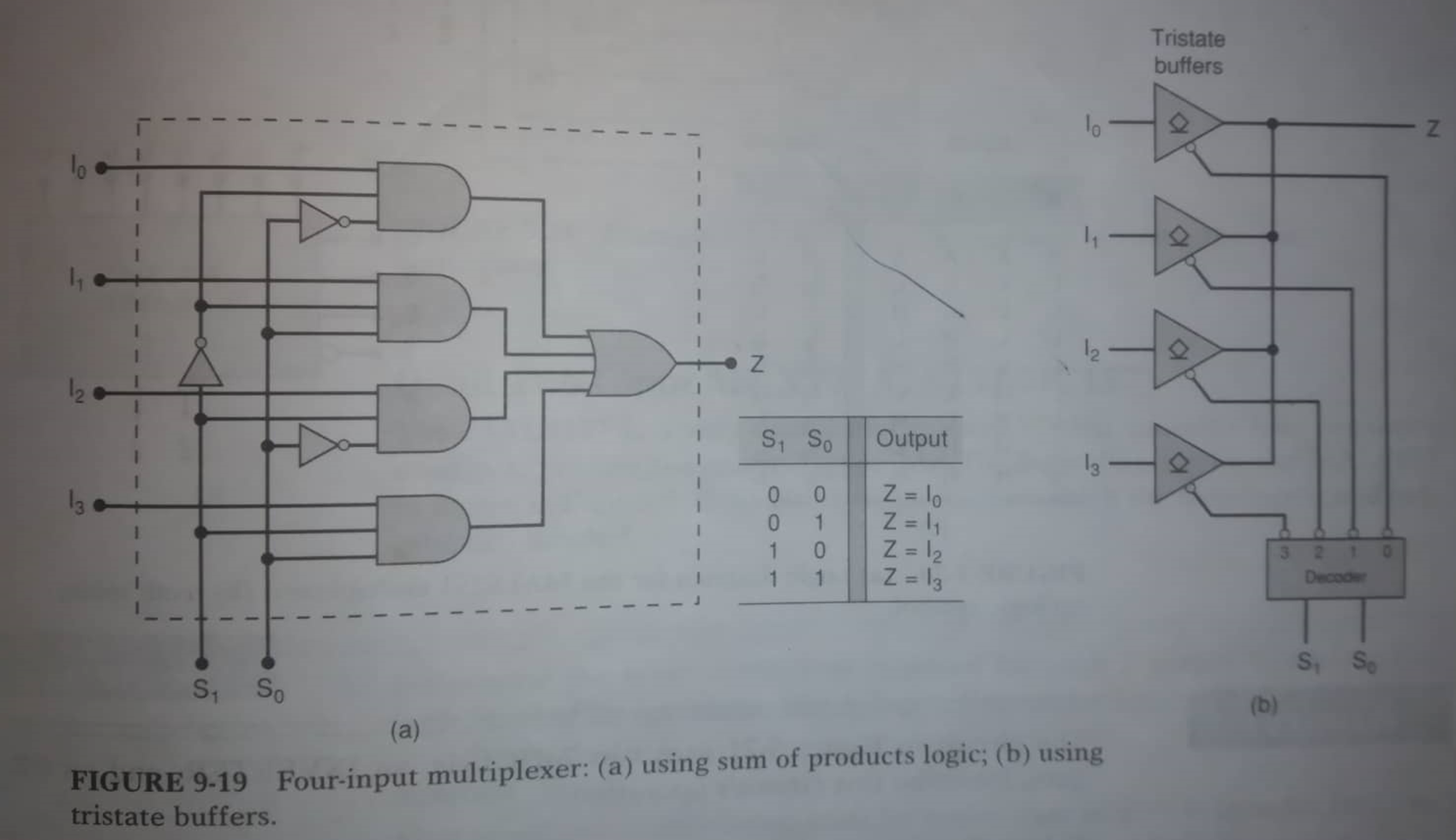
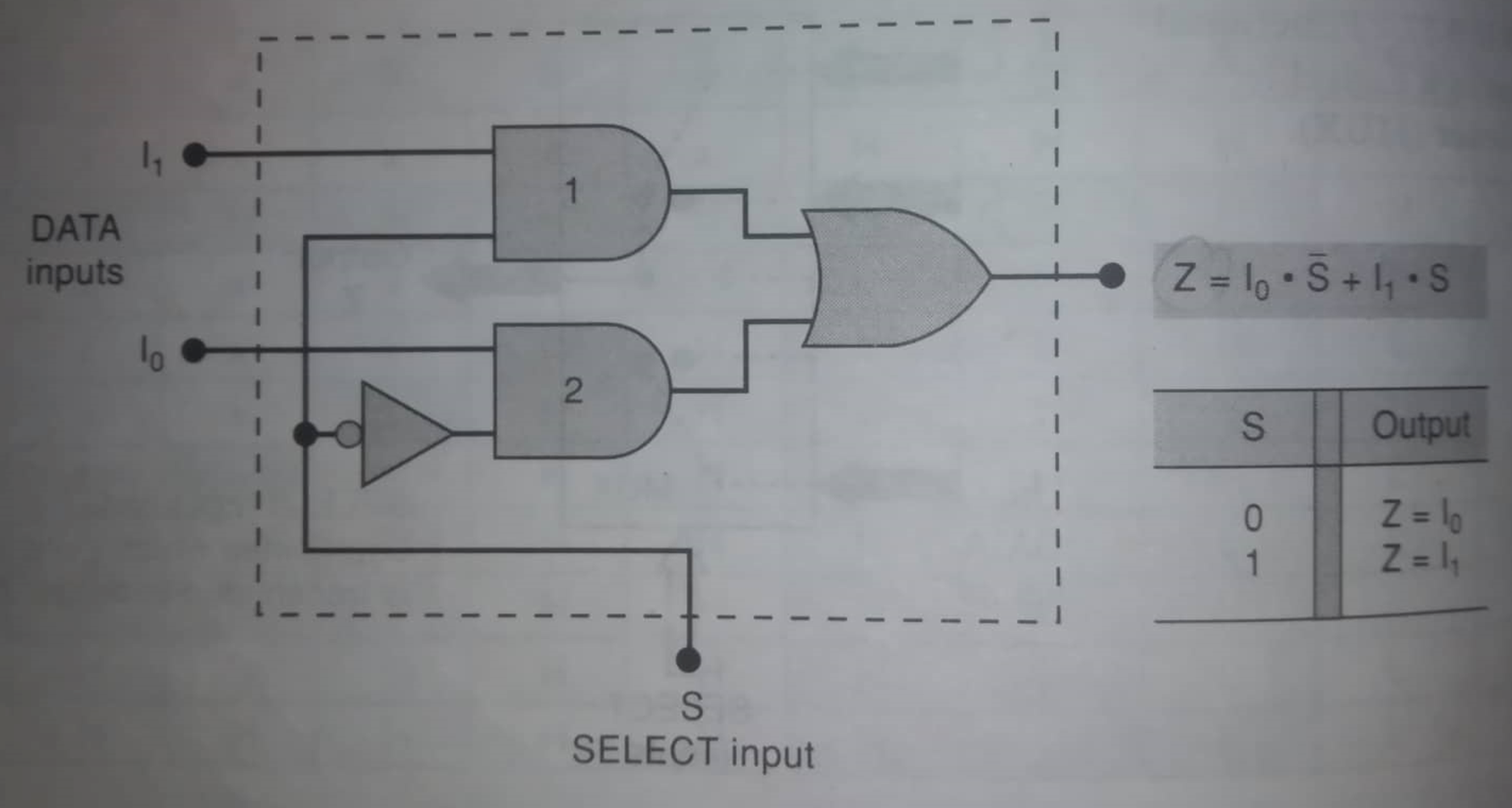
Multiplexer
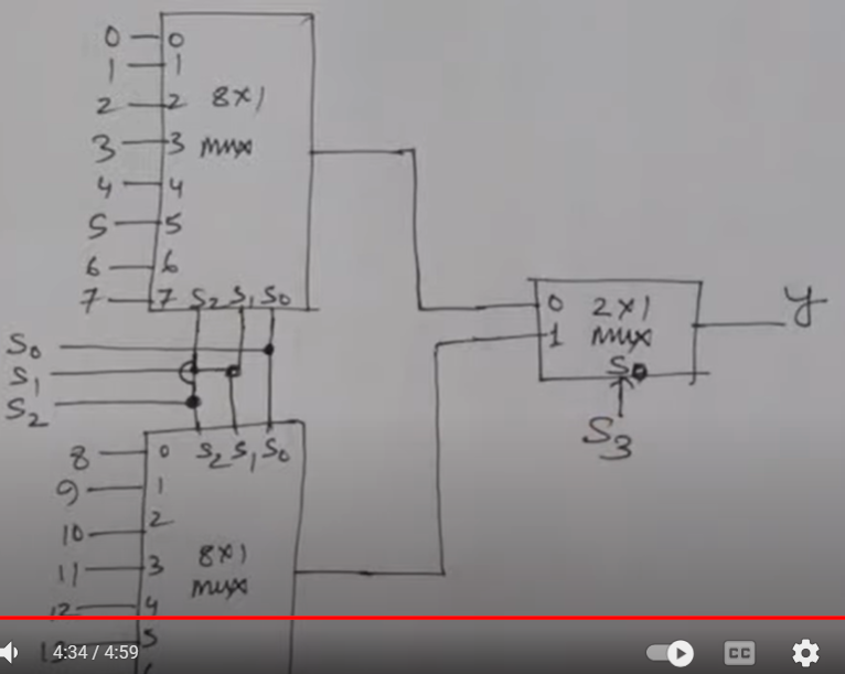
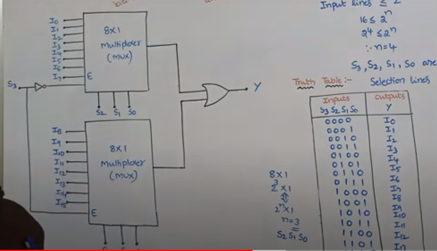
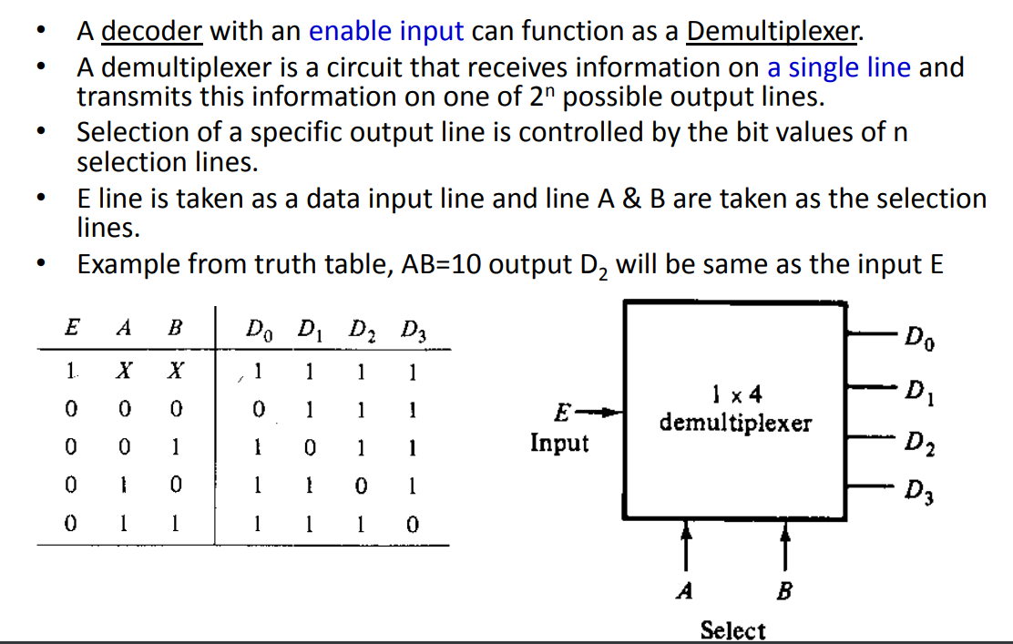
- What is multiplexer? Explain how two 8-input multiplexer can be combined ta form a 16-
input multiplexer.A multiplexer, often abbreviated as "MUX," is a device used in digital electronics and telecommunications to combine multiple input signals into a single output signal.
- Explain the logic diagram of four-input multiplexer
- Describe the two input multiplexer.
- Draw 1 of 8 decoder and a demultiplexer using 74ALS138 IC
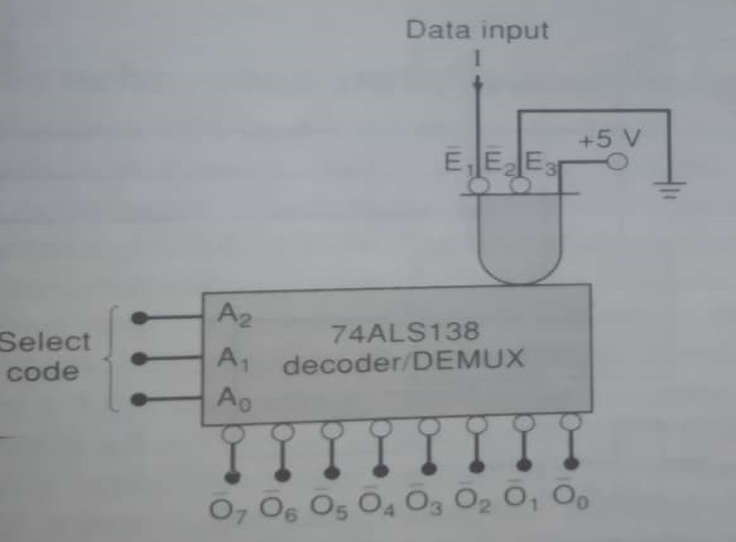
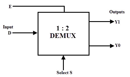
- Explain the logic diagram of 1-line-to-2-line demultiplexer.
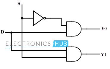
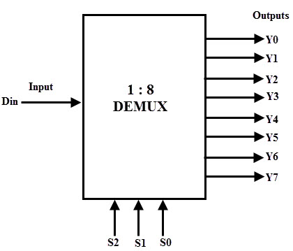
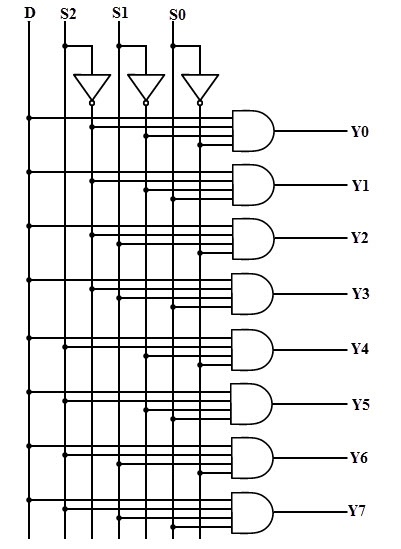
- Explain the logic diagram of 1-line-to-8-line demultiplexer.
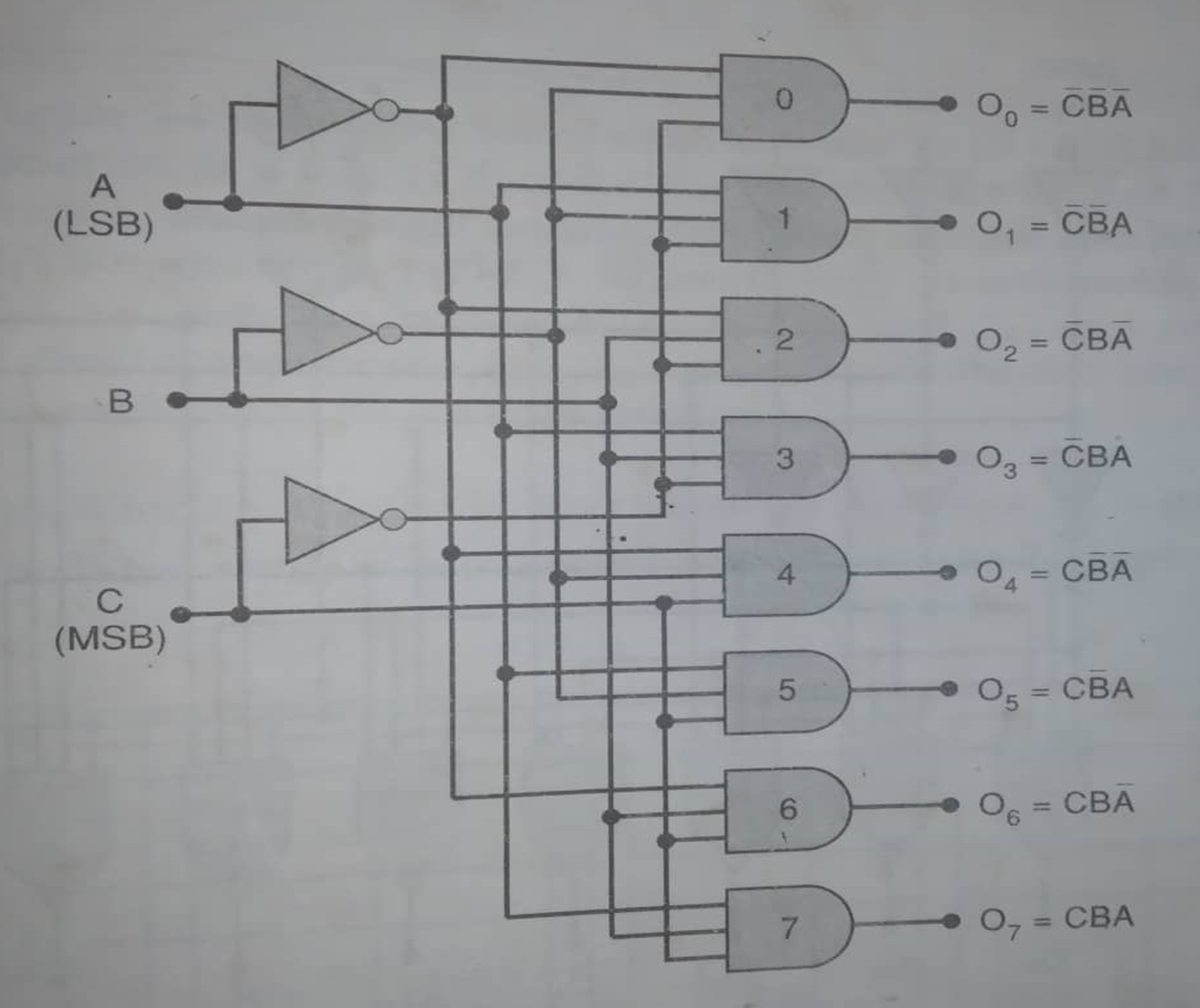
- Draw 1 of 8 Decoder
- Establish a comparison between multiplexer and de-multiplexer.
| Feature | Multiplexer | Demultiplexer |
|---|---|---|
| Purpose | Combines multiple input signals into one output | Splits one input signal into multiple outputs |
| Function | Selects one of the input lines based on control signals | Distributes the input signal to the selected output line based on control signals |
| Input Lines | Multiple input lines | Single input line |
| Output Lines | Single output line | Multiple output lines |
| Control Signals | Used to select the desired input line | Used to select the desired output line |
| Definition | A multiplexer, often referred to as a mux, is a digital circuit that combines multiple input signals into a single output line based on control signals. | A demultiplexer, often abbreviated as demux, is a digital circuit that takes a single input signal and distributes it to one of several possible output lines based on the control signals provided. |
- 4 to 1 line encoder
Some important notes:
- For Square wave the duty cycle is always 50%
- Assume that a five-bit binary counter starts in the 00000 state. What
will be the count after 144 input pulses?A:
Mod = 2^5 = 32
144%32 = 16 = 10000 (binary)
- In a ripple counter irrespective of the number of bits, each output waveform has
50% duty cycle
- For input multiplexer, select input required
- A certain semiconductor memory chip is specified as 2K8. How many words can be stored on this chip? What is the word size? How many total bets can this chip store?
Solution: 2K=2*1024= 2048 word.
Each word is 8 bit (one byte).
Total number of bits= 2048*8=16,384bits.
[1 K = 1024
1M = 1024*1024]
- Resolution
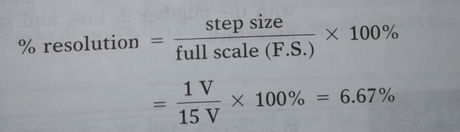
A 10-bit DAC has a step size of 10mV. Determine the full scale output voltage and the percentage resolution.
Solution:
No. of steps= 2^10-1=1023 steps of 10mV each.
So the full scale output= 10mV×1023= 10.23V
%resolution= 10mV/10.23V × 100% = 0.1%
- ADC/DAC
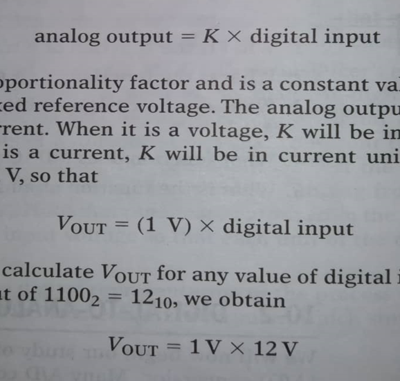
- A 5-bit DAC has a current output. For a digital input of 10100, an output current of 10 mA is produced. What will IOUT be for a digital input of 11101?
Solution: 10100= 20
IOUT =10 mA
Proportionality factor= 0.5
[K=10mA/20=0.5mA or 20×0.5mA=10 mA]
Now, 11101=29
IOUT= 29×0.5= 14.5 mA
- If asked for the largest input/output → 11111 = 31 (5 bit)
- 3 excess code
BCD code of the Number + 0011 = 3 excess code
- Binary to Gray Code
- MSB = MSB
- th bit = (
(Start from right, not mandatory)
- Gray to Binary Code
- Write the MSB , SUM = MSB
- bit = SUM + bit
- SUM = bit (Neglect the carry)
- Comparison between Encoder and Decoder
| Aspect | Encoder | Decoder |
|---|---|---|
| Purpose | Converts input data into a compressed representation or code. | Reconstructs the original input data from the compressed representation or code. |
| Input | Raw data or information to be encoded. | Encoded representation or code to be decoded. |
| Output | Encoded representation or code. | Decoded output, which is a reconstruction of the original input data. |
| Functionality | Extracts relevant features and patterns from the input data. | Utilizes the encoded representation to reconstruct the original data. |
| Architecture | Typically involves layers such as convolutional layers, pooling layers, and fully connected layers. | Often mirrors the architecture of the encoder but in reverse order. |
| Training | Trained using unsupervised learning techniques like autoencoders or generative models. | Trained alongside the encoder using the same dataset and loss function. |
| Applications | Image and video compression, anomaly detection, feature extraction. | Image and video reconstruction, machine translation, text generation. |
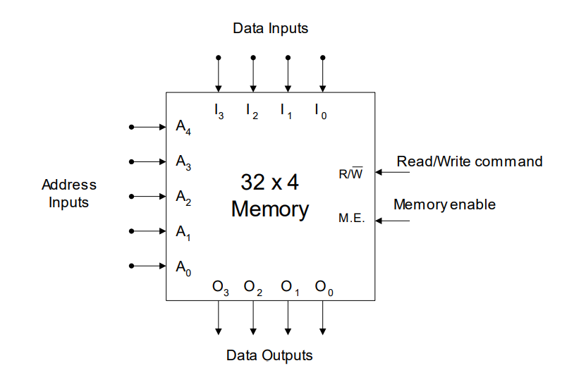
- 32X4 and 64X4 RAM internal organization
| 64x4 RAM | 32x4 RAM | |
|---|---|---|
| Number of Address Lines | 6 | 5 |
| Number of Data Lines | 4 | 4 |
| Number of Memory Locations | 64 | 32 |
| Number of Bits per Location | 4 | 4 |
| Address Decoder | Decodes 6 address lines to select one of 64 memory locations | Decodes 5 address lines to select one of 32 memory locations |
| Storage Cells | Consists of 64 storage cells, each capable of holding 4 bits of data | Consists of 32 storage cells, each capable of holding 4 bits of data |
| Read/Write Control | Determines whether to read or write data from/to the selected memory location | Determines whether to read or write data from/to the selected memory location |
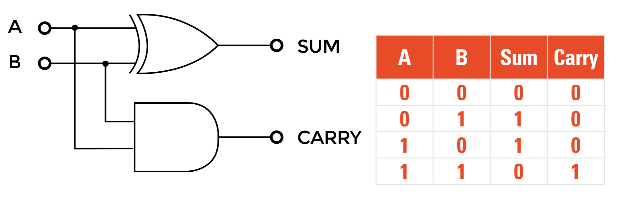
- Half adder
A Half Adder is a combinational circuit that adds two single-bit binary numbers (A and B) and produces two outputs: the sum (S) and the carry (C).
Sum =
Carry =
- Full Adder
A Full Adder is a combinational circuit that adds three single-bit binary numbers: A, B, and a carry input (C ), and produces two outputs: the sum (S) and the carry (C_out).
Carry =
Sum =
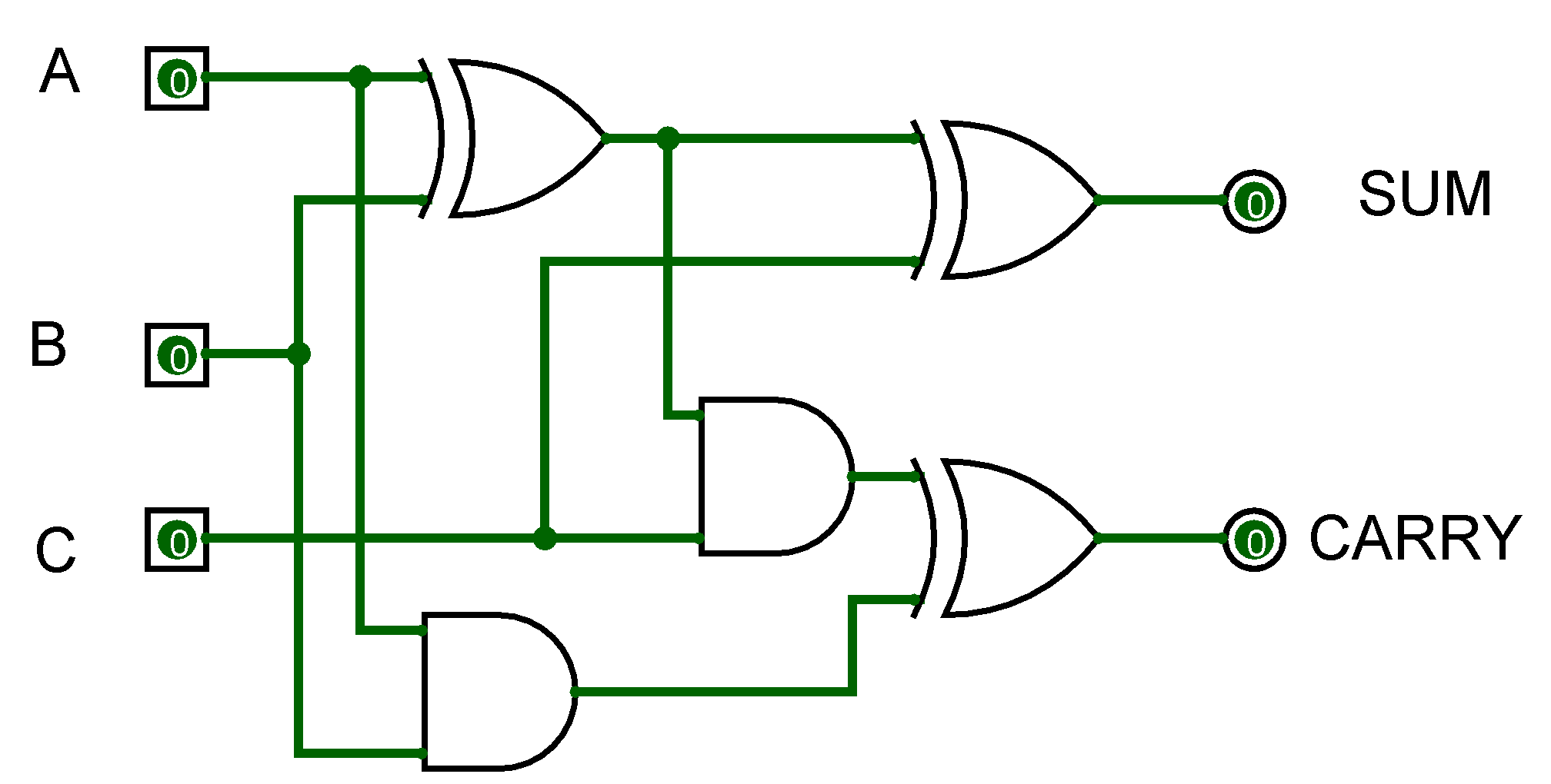
| A | B | C | SUM | Carry |
|---|---|---|---|---|
| 0 | 0 | 0 | 0 | 0 |
| 0 | 0 | 1 | 1 | 0 |
| 0 | 1 | 0 | 1 | 0 |
| 0 | 1 | 1 | 0 | 1 |
| 1 | 0 | 0 | 1 | 0 |
| 1 | 0 | 1 | 0 | 1 |
| 1 | 1 | 0 | 0 | 1 |
| 1 | 1 | 1 | 1 | 1 |
- Even Parity Generator :
- Odd Parity Generator : Where,
- Even Parity Checker : , = Parity Bit
- Odd Parity Checker :
- Ripple Up Counter
- Ripple Down Counter
- Decoder as Demultiplexer
- What are the differences between combinational and sequential circuits?
| Combinational Circuits | Sequential Circuits | |
|---|---|---|
| Feedback | No feedback involved | Feedback is involved |
| Memory | No memory | Has memory |
| Output | Depends only on current inputs | Depends on current inputs and past history |
| Design Complexity | Easier | Complex |
| Operation | Performs logic operations such as addition, subtraction, etc. | Builds memory elements, counters, shift registers, etc. |
| Examples | Logic gates, multiplexers, decoders, adders | Flip-flops, registers, memory units, counters, etc. |
- 16x4 ⇒ 32x4
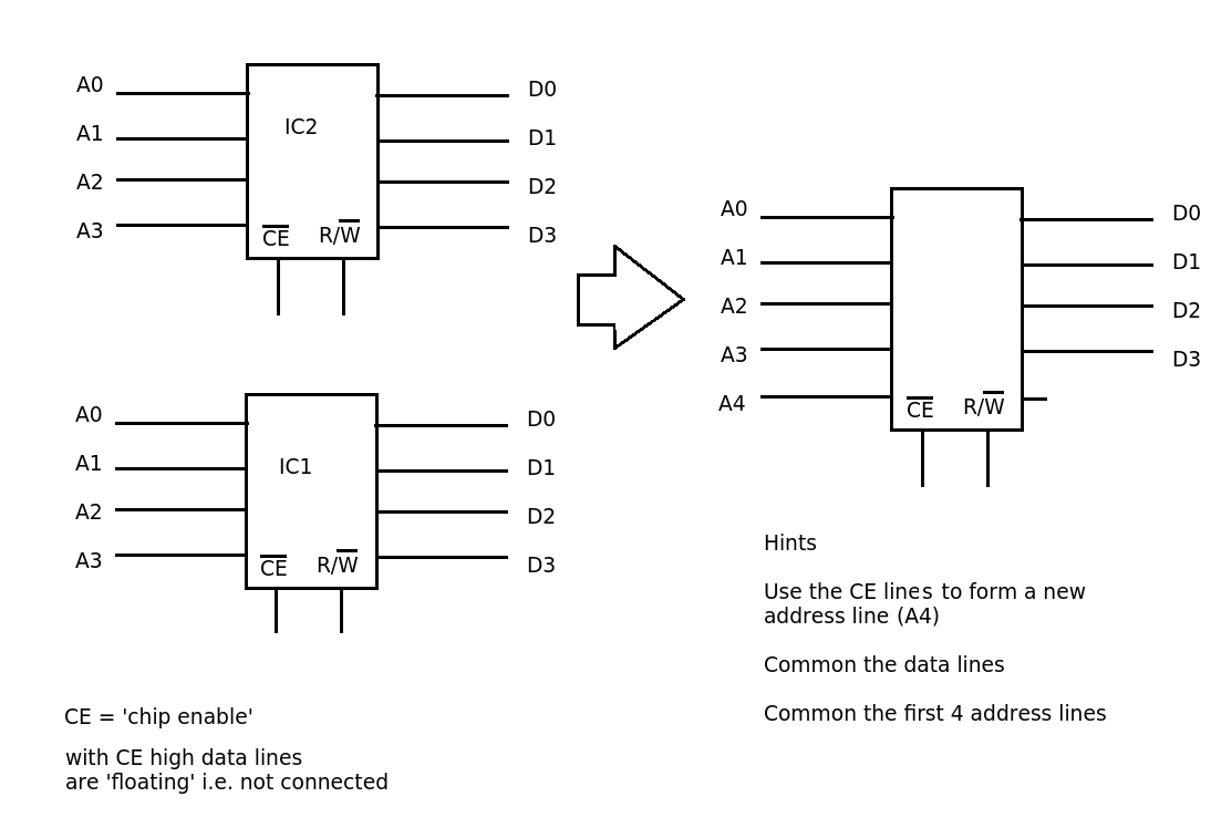
- Gather the necessary components
- Gather the necessary components
- Connect the address lines
- Connect the data lines
- Connect the control signals
- Mount the chips
- Verify connections
- Test the memory
- RAM block Diagram
CT 01 & Random :
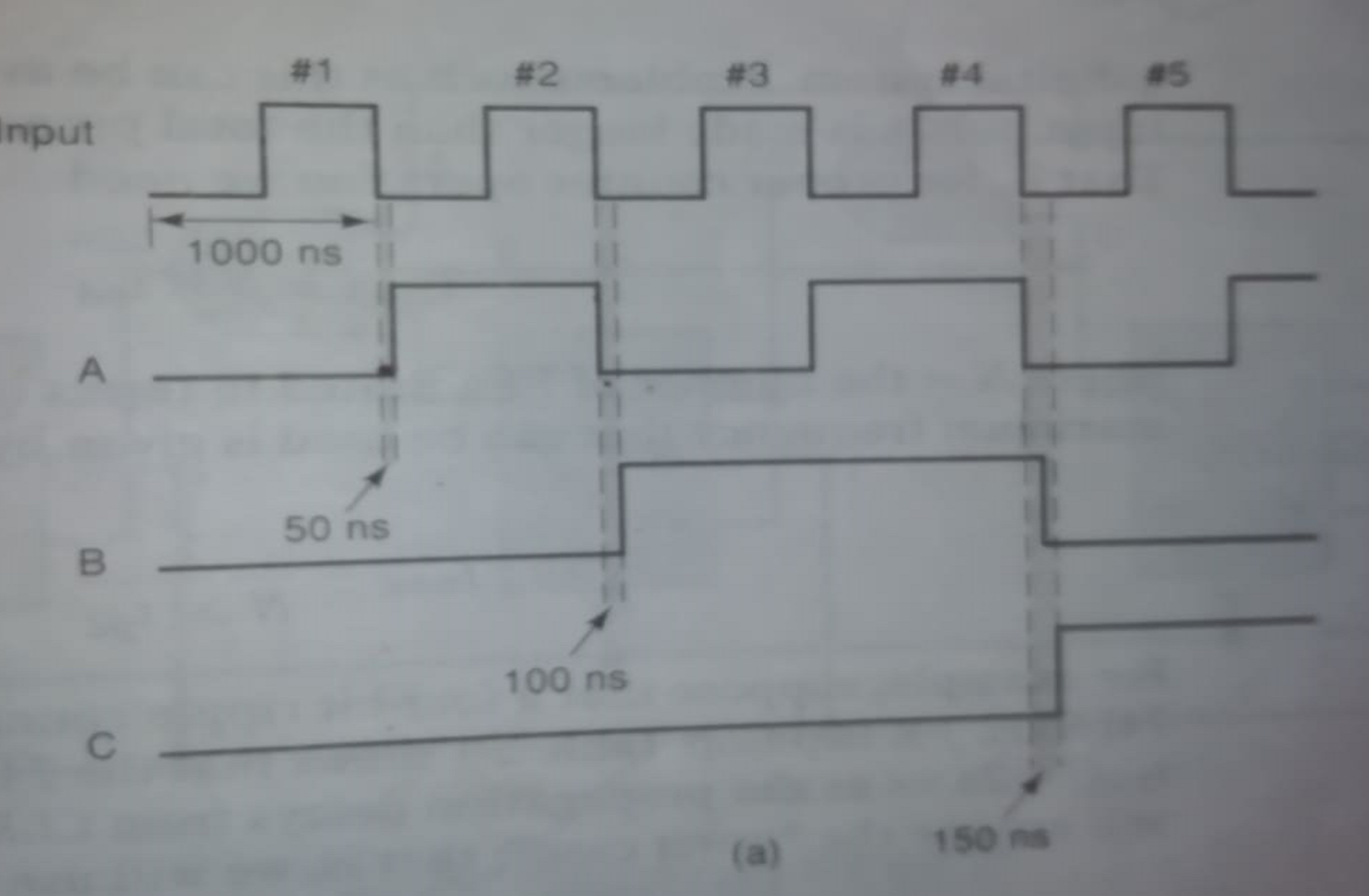
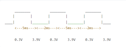
- Draw the timing diagram for a signal that alternates between 0.3V (binary 0) for 5ms and 3.9 V (binary 1) for 2ms
- What is the weight of MSB of 16-bit number?
- What is the weight of LSB of 16-bit number?
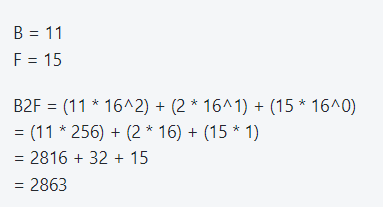
- B2F to Decimal
Keynote:
Number System Conversion
Any to Decimal →
Decimal to Any →
- Four numbers in HEX counting after E9D
E9E, E9F, EA0, EA1..
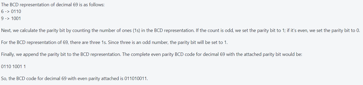
- Attach an even parity for bit to the BCD code for decimal 69
- Why can't parity method detect a double error transmitted data ?
- Single-bit Error: The even parity method can detect single-bit errors because any change in a single bit will result in an odd number of 1s, which will cause the parity check to fail. This allows for the detection of errors during transmission.
- Double Errors: However, if two bits are flipped (a double error), it is possible for the resulting pattern to have the same parity as the original correct data. For example, let's say the original data had even parity, and two bits were inverted, resulting in another valid pattern with even parity. In this case, the parity check will not detect the double error because the total number of 1s remains even.
Since the parity method checks for odd or even parity based on a count of 1s, it cannot differentiate between a correct pattern and certain combinations of double errors that maintain the same parity. This limitation makes the parity method ineffective at detecting such multiple errors.
Simplification of Expressions
1. De Morgan's theorem for three variables: (x + y + z)' = x'y'z' and (xyz)' = x' + y' + z'
K-map
CT 02:
- If the input frequency is 50HZ how much frequency will be produced by MOD-50 counter?
A: 1Hz [Topic : Frequency Division]
- How many AND gates are required to decode completely all of the states of a MOD-32 binary counter?
A: 32 , because 32 output states needed (AND gate only use in there) [Topic : Decoder]
- What are the inputs to the gate that decodes for the count of 21? (MOD-32)
A: The Decoder has 5 (why 5? 2^5 = 32) input. (A0(LSB), A1, A2, A3. A4(MSB))
21 binary Form = 10101, A0=1, A1=0, A2=1, A3=0, A4=1
- For an 8 input multiplexer, how many select inputs may require?
A: 3 , [Multiplexer has inputs, than select input/control : ]
- A counter is needed that will count the number of vehicles passing a road. A signal generator
generates a single pulse when each vehicle crosses the path. Note that the counter must be able to count as many as 5000 vehicles. How many FFs are required?A: Binary form of 5000 : 1001110001000 (13 bits), so 13 FF is needed