DEPT : Revision Purpose (Logic Family, Memory System, OP-Amp, Clipper-Clamper)
| Created by | Borhan |
|---|---|
| Last edited time | |
| Tag |
Lecture 1 to 3 :
Logic Families : TTL NOT*, NAND***, and CMOS*, CMOS NOT Gate, TTL and CMOS Tri-static logic, Totem-pole**, definitions and differences*
Questions:
- Draw and explain the working principle of a TTL NAND gate.
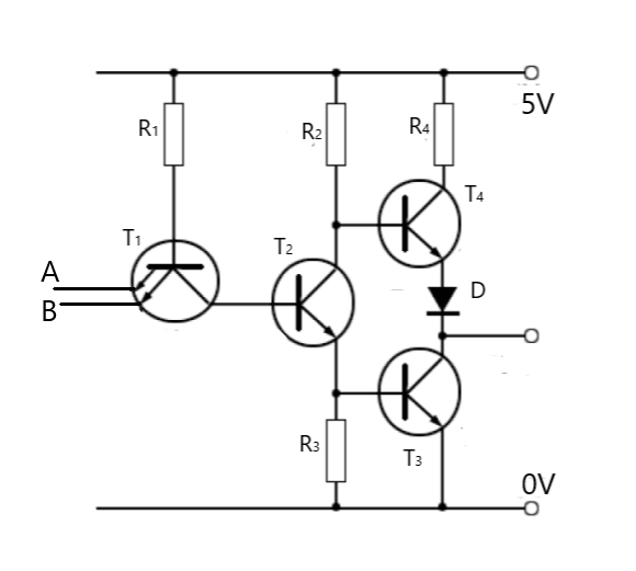
If both A and B is logic 1, the emitter-base junction of T1 would be reverse biased, while the collector-base junction would be forward biased due to sufficient voltage through R1, thereby turning on T2. The voltage drop across the emitter-base junction of T2 is adequate to activate T3, resulting in the activation of T1, T2, and T3. Conversely, the voltage drop across the emitter-base junction of T4 is approximately 0.9 (0.7+0.2=0.9, considered as 0.7 by Sir), which is insufficient (≥1.4 required) to activate T4, resulting in T4 remaining off. Consequently, the output will be logic 0, as T3 and V0 (output) are now short-circuited.
If either A or B are logic 0, the emitter-base junction of T1 would be forward biased, while the collector-base junction would be reverse biased, causing T2 and T3 to turn off. However, there will be sufficient voltage to activate T4 (≥1.4), leading to the activation of T4 and short-circuiting of the output terminal with T4. Hence, the output will be logic 1 (5 - 0.7*2 = 3.6 Volts).
| A | B | Y |
|---|---|---|
| 0 | 0 | 1 |
| 0 | 1 | 1 |
| 1 | 0 | 1 |
| 1 | 1 | 0 |
- Explain the following TTL circuit by using the logic input either A=0, B=0 or A=1, B=1
The question is somewhat similar as above.
- Compare the properties of open collector TTL NAND gate with those of Totem-pole TTL NAND gate.
| Property | Open Collector TTL NAND Gate | Totem-Pole TTL NAND Gate |
|---|---|---|
| Output Configuration | Open collector output, requires external pull-up resistor | Totem-pole output with push-pull configuration |
| Output Voltage Levels | Lower output voltage levels (typically around 0.2V when low and Vcc when high) | Higher output voltage levels (close to Vcc when high and close to ground when low) |
| Output Impedance | High output impedance when high, low impedance when low due to pull-up resistor | Low output impedance when high, low impedance when low |
| Output Driving Capability | Can sink current but cannot source current, requires external pull-up resistor | Can both sink and source current, capable of driving loads directly |
| Noise Immunity | Better noise immunity due to open collector configuration | Slightly less noise immunity compared to open collector configuration |
| Speed | Generally slower due to higher output impedance | Generally faster due to lower output impedance |
| Circuit Complexity | Simpler circuit design with fewer components | More complex circuit design with additional transistors for totem-pole output |
| Applications | Suitable for applications requiring wired-OR configurations | Suitable for general-purpose applications requiring both sinking and sourcing of current |
| Power Consumption | Lower power consumption due to open collector configuration | Slightly higher power consumption due to additional transistors and push-pull configuration |
- Why the Totem-pole output of TTL NAND gate cannot be tied together?
Because of current spike problem.
The active pull-up or totem-pole output of the TTL gate always has one transistor cutoff and the other turned on. We can not connect two outputs together. If one is trying to pull the output high, the other is trying to pull it low. We will have a very low impedance path to ground and very large current. For the same reason, the output must not be connected to any voltage source or to ground through a low impedance path.
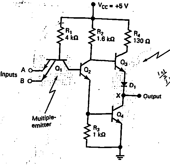
- Draw the circuit of TTL gate with Totem-Pole output.
Totem Pole means the addition of an active pull up the circuit in the output of the Gate which results in a reduction of propagation delay.
Logic operation is the same as the open collector output. The use of transistors Q4 and diode is to provide quick charging and discharging of parasitic capacitance across Q3. The resistor is used to keep the output current to a safe value.
- Explain the working principle of a TTL NOT gate.
When the input is low, the corresponding base-emitter junction is forward biased, and the base-collector junction is reverse biased. As a result transistor Q2 is cut off and also transistor Q4 is cut off. Transistor Q3 goes to saturation and diode D2 starts conducting and output is connected to Vcc and goes to logic high. Similarly, when input is at logic high, the base emitter junction is reverse biased, and the base-collection is forward biased.
There has enough voltage (≥1.4) to turn on Q2. Then Q2 turns on the Q4. But, Q3 goes to cutoff state because of having 0.7 (maybe 0.9) at the base-emitter junction. So, the output is connected with Q4 to GND and goes to logic low or 0.
- What is meant by 'Quantization error' of TTL device?
Quantization error in the context of TTL (Transistor-Transistor Logic) devices refers to the discrepancy between the ideal analog voltage levels and the discrete voltage levels that the TTL device can recognize or output.
- Mention the characteristics of TTL.
- Fan-in: The maximum number of inputs that the gate can handle.
- Fan-out: The maximum number of outputs a TTL gate can drive without affecting the gate’s performance. (Typically, its 10)
- Propagation delay: The time taken by the gate’s output to change state after the input changes. The delay for a typical TTL gate is about 10 ns.
- Powe Dissipation: It represents the amount of power needed by the device. The power dissipation TTL gate is about 10 mW.
- Noise Margin: It represents the maximum amount of noise voltage allowed at the input, which doesn’t affect the standard output. TTL gates allow a noise margin of about 0.4 volts.
- Temperature range: This is the range of safe operating temperature allowed for the gate. Standard 7400 family TTL gates have a temperature range from 0 to 70 degrees Celsius;
- What is meant by 'Fan out' of TTL device?
The maximum number of outputs a TTL gate can drive without affecting the gate’s performance. (Typically, its 10)
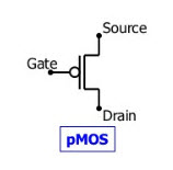
- Explain the CMOS logic gate.
The term CMOS stands for “Complementary Metal Oxide Semiconductor”. Complementary Metal Oxide Semiconductor transistor consists of P-channel MOS (PMOS) and N-channel MOS (NMOS).
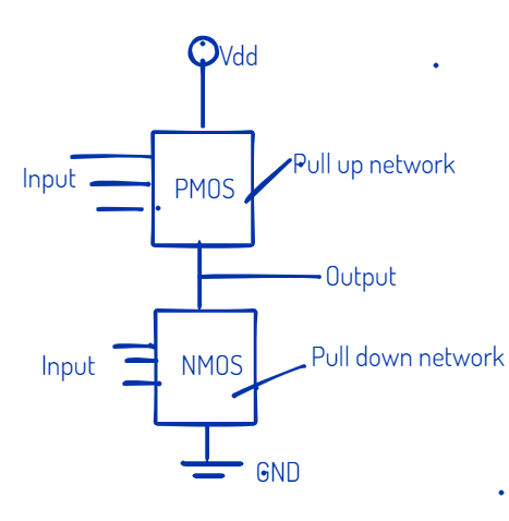
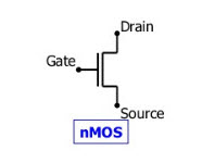
NMOS is built on a p-type substrate with n-type source and drain diffused on it. The majority carriers are electronics. When a high voltage is applied, it will conduct otherwise not.
PMOS consists of P-type source and drain diffused on a n-type substrate. Majority carriers are holes. When a high voltage is applied to he gate, the PMOS will not conduct, otherwise it will.
- What are the basic differences between TTL and CMOS signals?
| Specifications | TTL | CMOS | ECL |
|---|---|---|---|
| Basic Gate | NAND | NOR/NAND | OR/NOR |
| Components | Passive Elements & Transistors | MOSFETs | Passive Elements & Transistors |
| Fan-out | 10 | >50 | 25 |
| Noise Immunity | Strong | Extremely Strong | Good |
| Noise Margin | Moderate | High | Low |
| TPD in ns | 1.5 to 30 | 1 to 210 | 1 to 4 |
| Clock Rate in MHz | 35 | 10 | >60 |
| Power/Gate in mWatt | 10 | 0.0025 | 40 to 55 |
| Figure of Merit | 100 | 0.7 | 40 to 50 |
- Compare the properties of a CMOS/MOSFET switch with those of a BJT switch.
| Property | CMOS/MOFET Switch | BJT Switch |
|---|---|---|
| Operating Principle | Utilizes complementary pairs of MOSFETs For MOSFET: Metal-oxide semiconductor field | Utilizes bipolar junction transistors (BJTs) |
| Voltage Operation | Operates with both positive and negative voltages | Requires a positive voltage for operation |
| Power Consumption | Generally lower power consumption | Typically higher power consumption |
| Speed | Faster switching speed | Slower switching speed |
| Noise Immunity | High noise immunity due to low output impedance | Susceptible to noise due to high output impedance |
| Voltage Drop | Minimal voltage drop | Moderate voltage drop |
| Fabrication | Typically fabricated using CMOS technology | Fabricated using semiconductor processes |
| Input Impedance | High input impedance | Moderate input impedance |
| Output Impedance | Low output impedance | Moderate output impedance |
| Temperature Sensitivity | Low sensitivity to temperature variations | Moderate sensitivity to temperature variations |
| Area Occupancy | Requires larger silicon area | Requires smaller silicon area |
- Write the various characteristics of MOS logic gates regarding speed, power utilization and packing density.
| Characteristic | Speed | Power Utilization | Packing Density |
|---|---|---|---|
| NAND Gates | Fast | Moderate to Low | High |
| NOR Gates | Fast | Moderate to Low | High |
| NOT Gates | Fast | Low | High |
| AND Gates | Moderate | Moderate to Low | Moderate to High |
| OR Gates | Moderate | Moderate to Low | Moderate to High |
| XOR Gates | Moderate | Moderate to Low | Moderate to High |
| XNOR Gates | Moderate | Moderate to Low | Moderate to High |
- Write the name of 5 logic families.
- TTL (Transistor-Transistor Logic)
- CMOS (Complementary Metal-Oxide-Semiconductor)
- ECL (Emitter-Coupled Logic)
- RTL (Resistor-Transistor Logic)
- NMOS (N-type Metal-Oxide-Semiconductor)
- DTL (Diode-Transistor Logic)
- CTL (Complementary Transistor Logic)
- NMOS Inverter
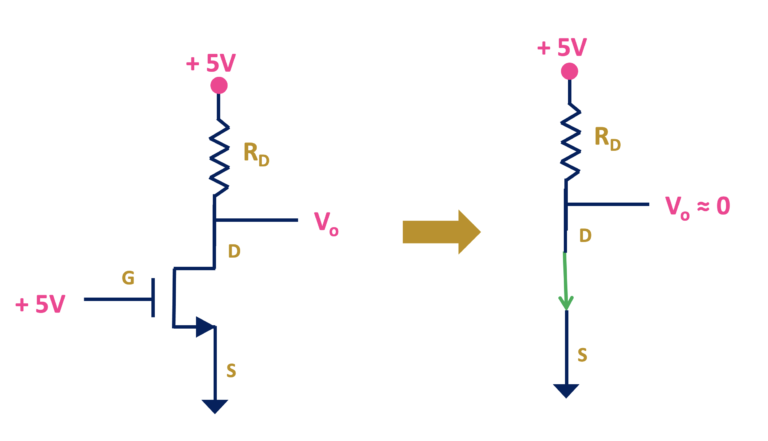
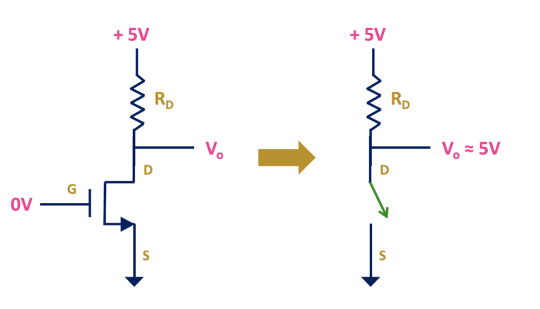
Let’s assume that the threshold voltage (VT) of the NMOS transistor is 0.5 V. When VGS = 5V or when VGS > VT , (Let’s assume that logic ‘1’ is 5V) then MOSFET will be ON and acts as a close switch. Therefore, in actual case also, the output will be very close to 0V or logic ‘0’.
Similarly, when VGS = 0V or logic ‘0’ then MOSFET will be OFF and it will act as a open switch. And through the drain resistor, the output will get connected to the supply voltage. That means when input is 0 then output is VDD.
Out of Question
CMOS inverter/NOT gate
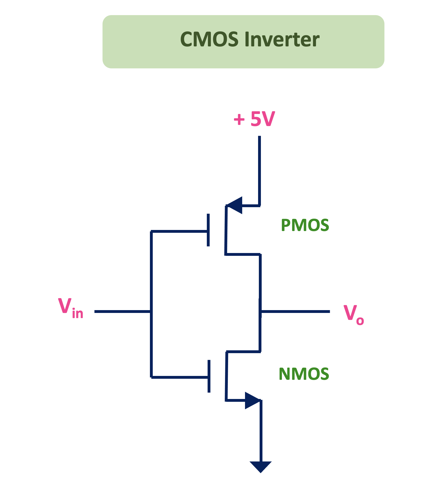
Vin is logic ‘0’, then PMOS will be ON and NMOS will OFF.
Vin is logic ‘1’, then PMOS will be OFF and NMOS will ON.
TSL inverter/Tri Static TTL inverter
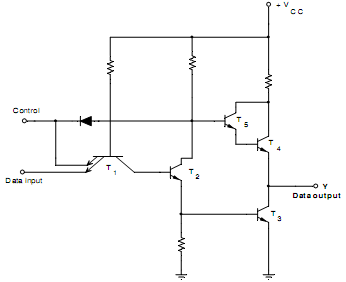
| Data Input | Control | Data Output |
|---|---|---|
| 0 | 0 | High - Z |
| 1 | 0 | High - Z |
| 0 | 1 | 1 |
| 1 | 1 | 0 |
CMOS Tri-state inverter
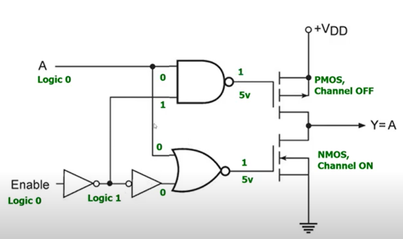
| E | A | Y |
|---|---|---|
| 0 | 0/1 | A |
| 1 | 0/1 | High-Z |
Lecture 4 to 5
Topic: RAM, ROM classifications*, comparisons*, designing RAM***, ROM*
- Design a 32x4 RAM combining two 16x4, RAMs and derive operations.
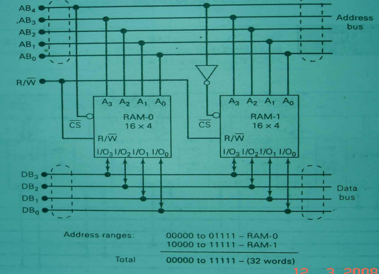
| CS | R/W | Mode | Data pins |
|---|---|---|---|
| 0 | 1 | Read | Data out |
| 0 | 0 | Write | Data in |
| 1 | X | Standby | High Z |
- Design 16kx8 EEPROM and deduce with truth-table.
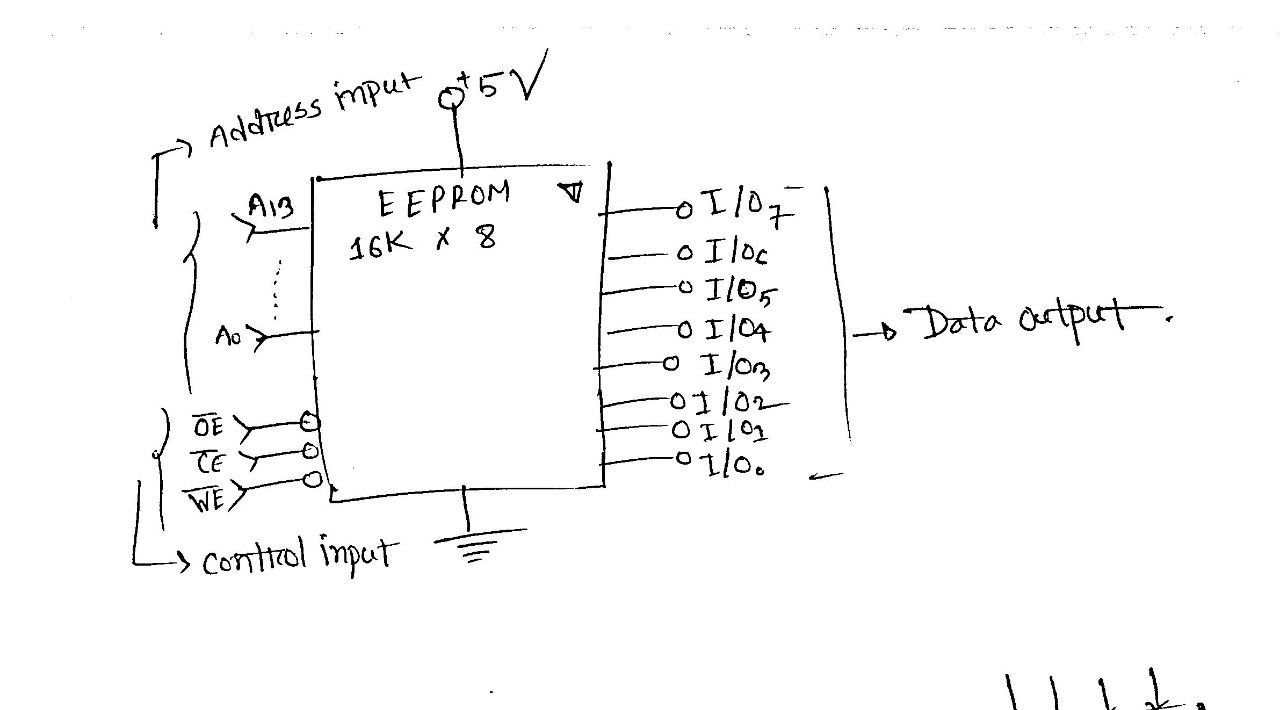
| MODE | CE | OE | WE | Data Pin |
|---|---|---|---|---|
| Read | 0 | 0 | 1 | Data Out |
| Write | 0 | 1 | 0 | Data in |
| Standby | 1 | X | X | High Z |
- Write the comparisons among MROM, EPROM and EEPROM.
| PROM | EPROM | EEPROM | Flash Memory | MROM |
|---|---|---|---|---|
| Programmable ROM | Erasable Programmable | Electrically Erasable Programmable | Flash Electrically Erasable ROM | Mask ROM |
| Not erasable | Erasable using UV light | Erasable electrically | Erasable electrically | No applicable |
| One-time programmable | Reprogrammable after using UV | Reprogrammable electrically | Reprogrammable electrically | Not programmable after manufacturing |
| Slow | Slower than EEPROM | Slower than Flash | Faster than EPROM and EEPROM | Fast |
| Density low | Low to medium | Low to medium | High | High |
| Cost low | Medium | Medium to high | Low to medium | Low |
- Explain 32x4 memory operation.
A 32x4 memory refers to a memory organization where there are 32 memory locations and each location can store 4 bits of data.
Address line = 2^5 = 5
Input and output line : 4
Operations:
- Addressing: To access a specific memory location we need 5 address lines to uniquely address each location.
- Read Operation: At first chip selector remains zero. Let address location is 11111 = data is . If , then input buffer inactive and output buffer is active.
Data input: XXXX
Address Line: 11111
R/W : 1
: 0 (always)
Output data:
- Write Operation: Let address location is 11111 = 31 and data is 1101. When R/W is 0, then input buffer is active and output buffer is active.
Data input: 1101
Address line:11111
R/W:0
: 0 (always)
Data output : XXXXX
- Data Output: After a read operation, the data stored at the specified memory location output through the data output lines. The data output will be 4-bit binary value representing the information.
- Data Input: During a write operation, the provided data that is to be stored at the specified memory location through the data input lines. The memory stores the provided data at the specific location.
- Design 64x4 RAM and define its READ and WRITE operations.
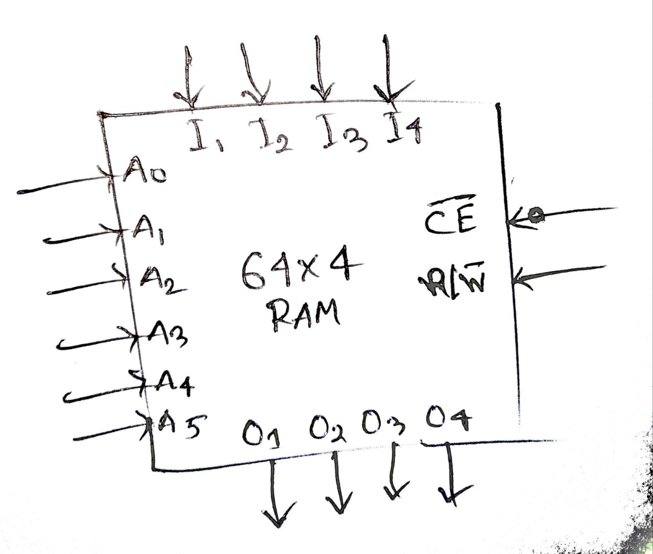
A 64x4 memory refers to a memory organization where there are 64 memory locations and each location can store 4 bits of data.
Address line = = 6
Input and output line : 4
- Read Operation: At first chip selector remains zero. Let address location is 1111111 = data is . If , then input buffer inactive and output buffer is active.
Data input: XXXX
Address Line: 1111111
: 1
: 0 (always)
Output data:
- Write Operation: Let address location is 111111 = 61 and data is 1101. When R/W is 0, then input buffer is active and output buffer is active.
Data input: 1101
Address line:111111
:0
:0
Data output : XXXXX
- Explain the architecture of static RAM.
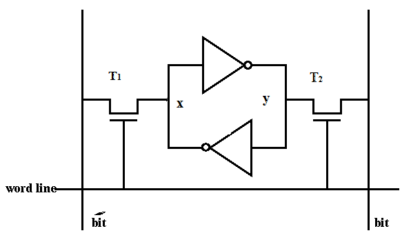
Static Random Access Memory (SRAM) is a type of semiconductor memory that uses bistable latching circuitry (flip flop) to store each bit of data/ It is fast and not require refreshing like DRAM.
The architecture of SRAM:
- Flip-flops: The basic building block of SRAM is the flip-flop and consists of cross coupled inverters that latch the input values. They can store one bit of data.
- Word and bit lines: Word lines are used to select a particular row of memory cells for reading or writing. Bit Lines are used to read the data stored in the selected or to write data into memory cells.
- Sense amplifier: Amplify voltage differences on bit lines for read operations.
- Address Decoders: Select memory cells based on provided address.
- Write Circuity : Store data into selected memory cells.
- Control Logic: Coordinates operations and ensure efficient memory access.
- Describe the conditions at each input and output when the data word 1110 is to be written into address location 01101
Reading (Extra/out of question)
Address input: 01101
Data Inputs: xxxx
: HIGH
Chip Select = LOW
Data outputs: 0001
Writing
Address input: 01101
Data Inputs: 1110
: LOW (0)
Chip Select = LOW (0)
Data outputs: xxxx (usually High Impedance)
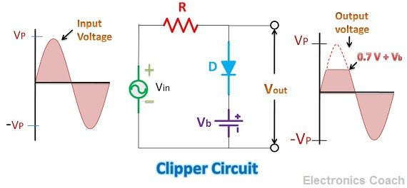
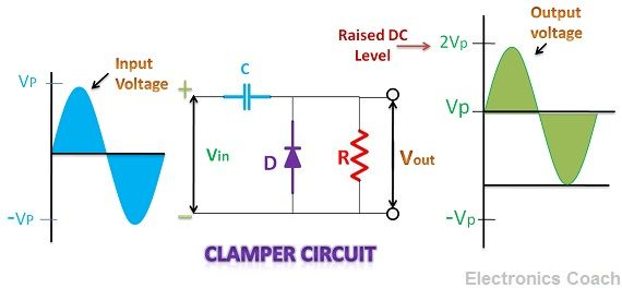
Clipper and Clamper Circuit
- Show the comparison between Clipper and Clamper circuits with appropriate figures
| PARAMETERS | CLIPPER | CLAMPER |
|---|---|---|
| Definition | Clipper delimit the amplitude of the output voltage by clipping that part without affecting the remaining part. | Clamper shifts the DC level of the output voltage either upward or downward depending on whether positive or negative clamper. |
| Output Voltage | Less than the input voltage. | Multiples of input voltage. |
| Energy storage component | Not required | Requires (Capacitor is used as energy storage element) |
| Shape of Output Waveform | Shape changes (Rectangular, sinusoidal, triangular etc.) | Shape remains same as input waveform. |
| DC Level | Remains same | DC level get shifted |
| Applications | In transmitters, receivers, amplitude selector, noise limiter etc. | In voltage multiplying circuits, Sonar, Radar system etc. |
- Design two simple clipper circuit when diode and resistor are interchanged and explain their operations./Draw and explain a clipper circuit to clip the positive half cycle of a sinusoidal signal.
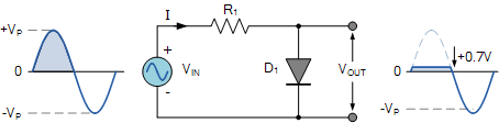
It clips the positive output voltage waveform.
When the positive half cycle is being passed, the diode is forward biased and the output voltage is zero because of being short-circuited the current doesn’t pass through output. Similarly, when the negative half cycle is being passed, the diode is reverse biased, so the output voltage is similar to the input, if we neglects the resistance.
It clips the positive output current waveform.
When the positive half cycle is passed, the diode is in reverse bias, and the voltage across is zero. Similarly, when the negative half cycle is passed, the diode is forward biased, so the voltage through is similar to the input voltage.
- Show the effect of RC time constant in a clamper circuit.
Clamper is the process of introducing a dc level into an signal. It is also known as dc restorers. The circuit contains a capacitor, a diode and resistor. In order to maintain the time period of wave form, the time constant must be greater than half the time period.
Time constant,
Where,
The time constant of charge and discharge of the capacitor determines the output of a clamper circuit.
In a clamper circuit a vertical shift of upward or downward takes place in the output waveform with respect to the input signal.
The load resistor and capacitor affect the waveform. So, the discharging time of the capacitor should be large enough. The DC component present in the input is rejected when capacitor coupled network is used. Hence, when dc needs to be restored, clamping circuit is used.
- Why should the RC time constant be large in a clamper circuit?
The RC time constant should be large in a clamper circuit because of maintaining the time period of the waveform.
Clamper is the process of introducing a dc level into an signal. It is also known as dc restorers. The circuit contains a capacitor, a diode and resistor element. The magnitude R and C to be use used in the clamper circuit must be chosen such than the time constant is larger enough to ensure that the voltage across the capacitor does not discharge significantly during the interval the diode is non conducting,
In a good clamper circuit, the circuit time constant should be at least ten times the time period of the input signal voltage.
So, it is clear that in order to maintain the time period of the wave form, the time constant must be greater than the half time period.
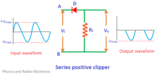
- Draw and explain a clipper circuit to clip the negative half cycle of a sinusoidal signal.
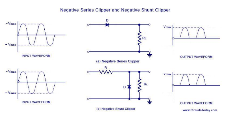
- Negative Series Clipper
- During the positive half cycle, the diode is forward biased and acts like a short circuit. So, the current pass through the . The output is similar to the input signal.
- During the negative cycle, the diode is reverse biased and acts as an open circuit. So, the current doesn’t pass through . The output is zero.
- Negative Shunt Clipper
- During the positive half cycle, the diode is reverse biased and behaves as an open circuit. Consequently, the entire input voltage appear across the load resistance .
- During the negative half cycle, the diode is forward biased and behaves as a short circuit. So, the voltage drop across a short circuit is zero. So, the voltage across is zero too.
- If V=50V P-P ; VB1=15V and VB2=15V of the following figure. Draw the output voltage Vo with appropriate figure and explain the circuit operations.
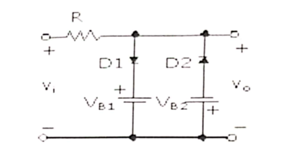
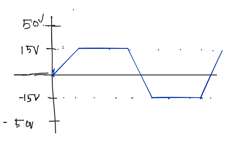
- During positive half-cycle ( will be always reverse biased)
- , the diode will be reversed biased. So, the output will be
- , the diode will be forward biased. So, the output will be
- During negative half-cycle ( will be always reverse biased)
- , the diode will be reversed biased. So, the output will be
- the diode will be forward biased. So, the output will be
OP-Amp
- Explain the Schmitt trigger circuit shown here.
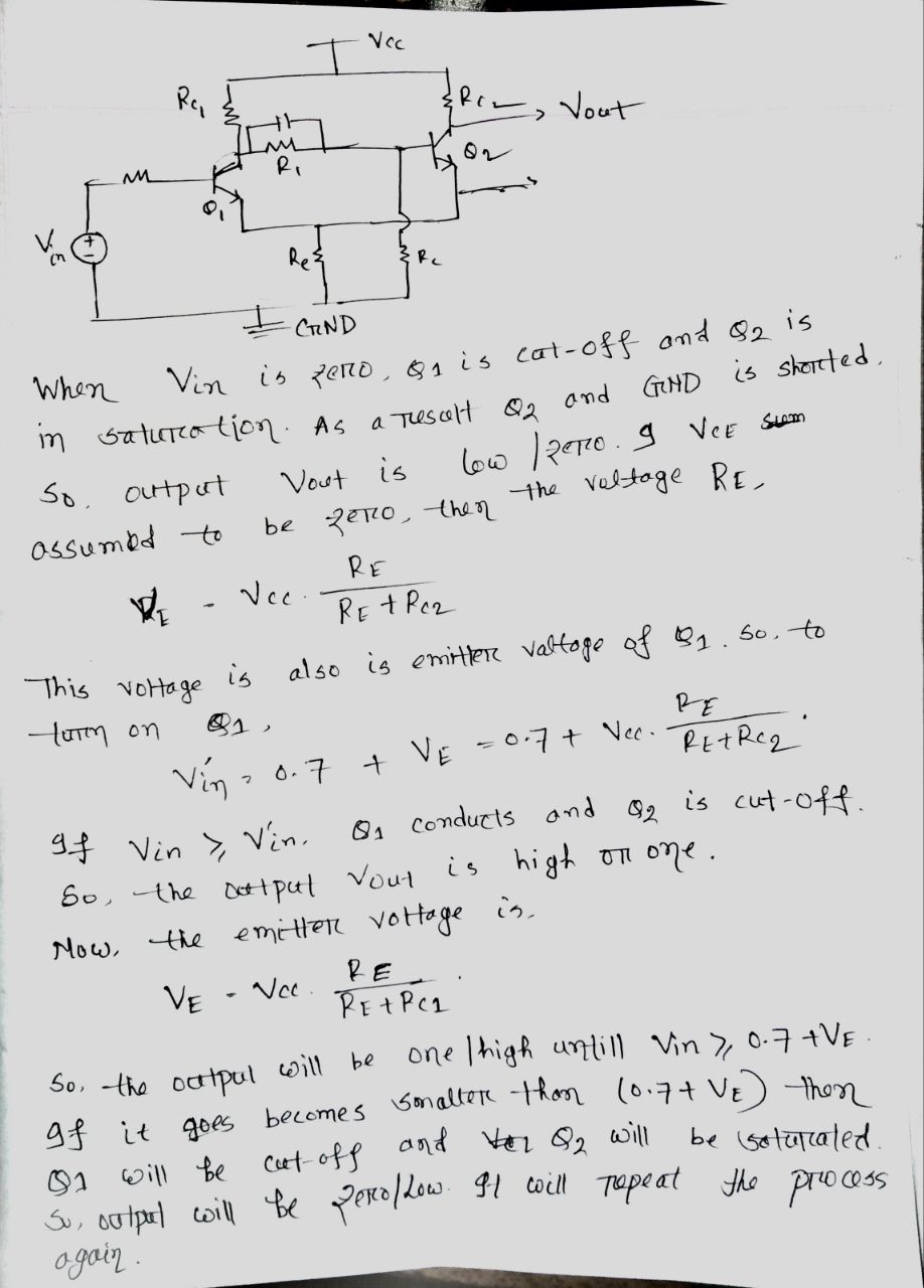
- By using an Op-Amp, design a relaxation oscillator to oscillate at the frequency of 10KHz
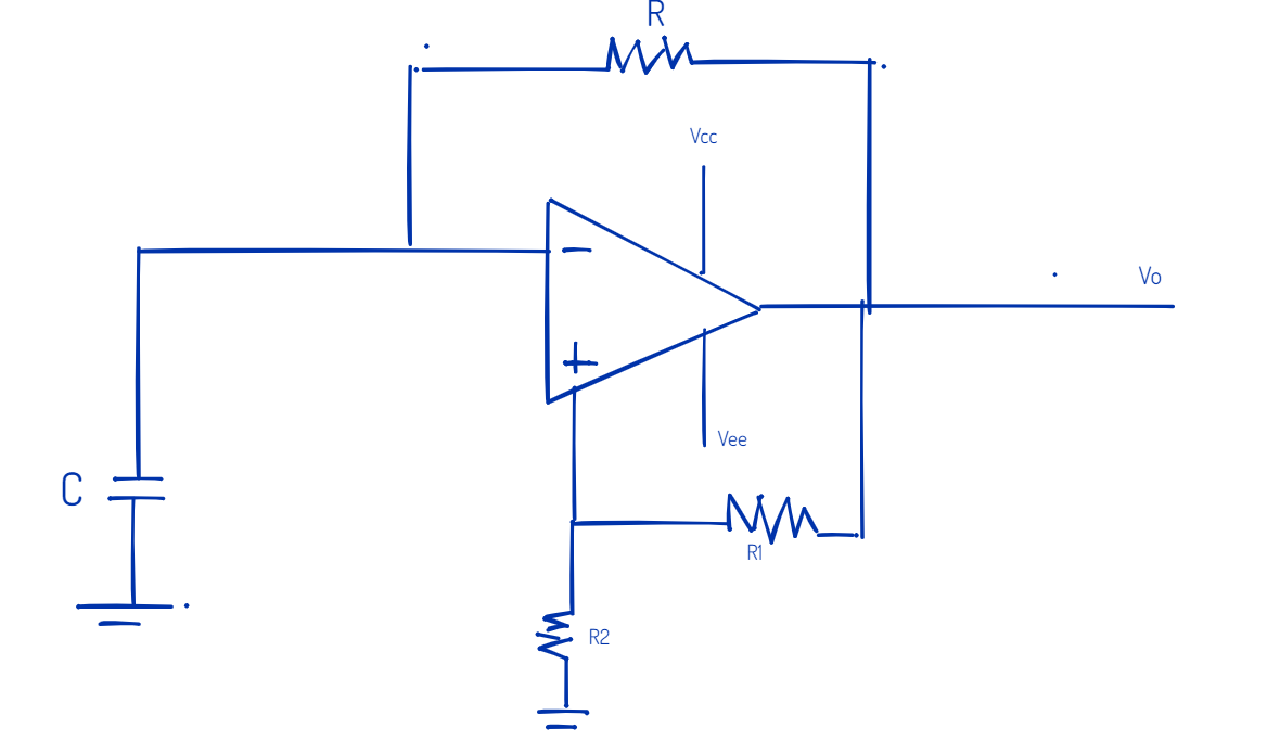
- Draw the charging and discharging waveforms the capacitor used in the relaxation oscillator by Op-amp.
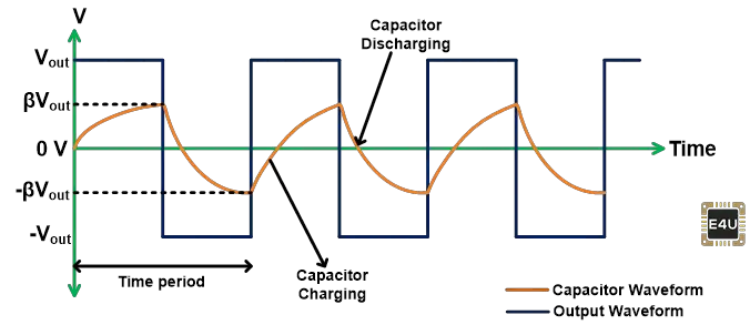
An OP-Amp relaxation oscillator is also known as an astable multivibrator. It is used to generate square waves. The circuit diagram the Op-Amp relaxation oscillator is shown in the figure
The capacitor will charge exponentially towards . It never reaches because when its voltage hits the UTP, the output then switches . Now a negative voltage is being feedback, so, the capacitor reverse its charging direction. The capacitor voltage decreases. When it hits the LTP, the output switches back to because of the capacitor output is rectangular wave.
- By using Op-amp, draw and explain a relaxation oscillator.
An op-amp relaxation oscillator is also known as astable multivibrator. It is used to generate square waves.
Assume that the output is in positive saturation. If and and the value of capacitor is less than these voltage, we will get positive voltage in output and a part of this voltage go through the resistors. When capacitor want to cross the voltage of resistor becomes negative, then the resistor voltage becomes negative. In this way, when the capacitor again become less than the voltage of resistor it the becomes positive again. In this way we get rectangular through this charging and discharging.
- Write down the general characteristics of Op-amp.
Characteristics of Op-amp:
- Input impedance is an infinite value
- Output impedance is very low
- Infinite open-loop gain
- Infinite bandwidth due to the ideal gain inside the op-amp
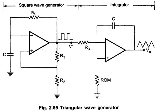
- By using an Op-amp, draw and explain a waveform converter circuit to produce triangular waveform pulses.
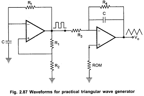
The output of a integrator is a triangular wave if input is a square wave. Here, we are converting a wave into square by using relaxation oscillator.
Converting to Square wave: …
Converting Square to Triangular: Basically triangular wave is generated by alternatively charging and discharging a capacitor with a constant current. This is achieved by connecting integrator circuit at the output of square wave generator. Assume, that V’ is high at +Vsat . This forces a constant current (+Vsat/3) through C to drive Vo negative linearly. When V’ is low at Vsat it forces a constant current (-Vsat/3) through C to drive Vo positive, linearly.
- Describe one application of Schmitt triggers other than their use in relaxation oscillators.
…
- Draw and explain the working principle of a non-inverting amplifier with op-amp.
The non-inverting op-amp circuit diagram is shown below. The output voltage signal is given to the inverting terminal of the op-amp like feedback through a resistor where another resistor to the ground. These two resistors will provide necessary feedback to the operational amplifier. In perfect condition, op-amp’s input pin will provide maximum input impedance whereas the output pin will provide low impedance.
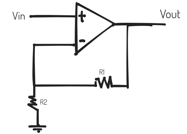
The current rule: No current flows into the input of the op-amp.
The voltage rule: The output of the op amp attempts to ensure that the voltage difference between the two inputs is zero.
- An op-amp relaxation oscillator has feedback fraction B=0.5, feedback resistor R=10 ohms and charging-discharging capacitor C=0.0022uF. What is the frequency of the output rectangular wave?
- By using an op-amp, draw and explain a waveform converter circuit to produce triangular wave from pulses.
- Draw and explain an op-amp Integrator circuit.
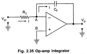
The output voltage is the integration of the input voltage. Here, the non-inverting is grounded and inverting connects with a resistor and a Capacitor which is connected with output too.
The note B is grounded so is A.
The current is flowing from to so
.. (ii), … (i)
- Draw and explain an op-amp Differentiator circuit..
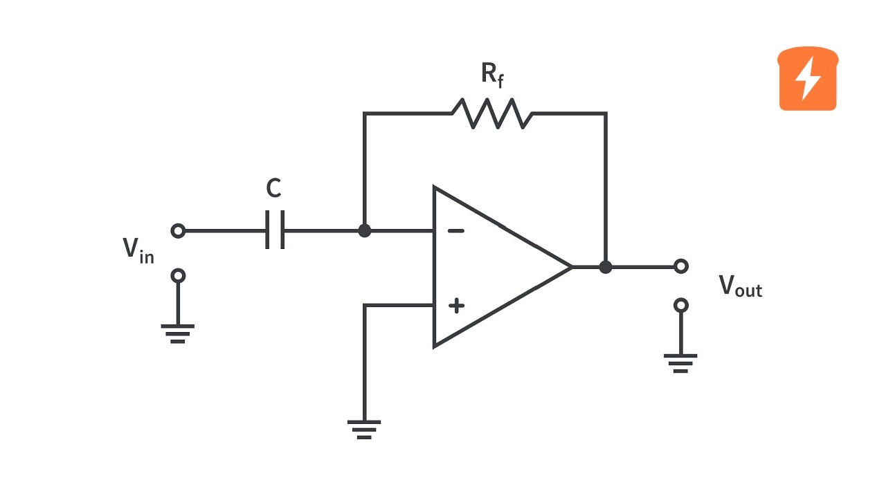

Now,
⇒
-
Multivibrator
- What is meant by 45% duty cycle? Explain with an example.
Duty Cycle: It is defined as the ratio of pulse width to the total time period. It can expressed in percentage also. In general Duty Cycle is nothing but fraction of total time during which the signal is High (ON).
45% duty cycle means that the signal active high for 45% of total time period.
⇒
⇒
The below graph showing that a signal or electronic switch is ON for 45% of it each time period.
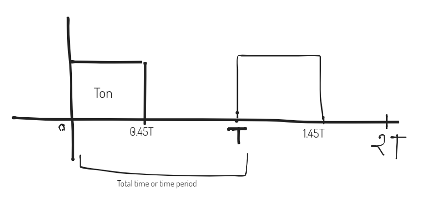
45% duty Cycle